4.1 Application overview
1 Background
In many data converter applications, a side effect of advances in converter technology is that device packages, power consumption and circuit board area are now driven by interconnect and data transfer requirements, instead of the intrinsic needs of the application. High resolution data converters typically need more board space for the interconnection (board traces and vias) than for the chip package itself. Single-ended digital interfaces cause switching noise, which affects the performance of the analog part, and parallel differential-signaling interfaces (such as LVDS) exacerbate the board area cost of the interconnect.
While technological advances have led to significantly lower power consumption in the intrinsic part of converters, similar reductions in the I/O power consumption and the size of the chip package have not taken place because of the large number of I/O lines needed. These problems become even more evident when multiple converters are integrated in the same package, e.g., for direct conversion radio transceivers. This I/O pin count limit also affects multi-channel data acquisition applications, such as beam forming, in which signal processors synthesize the output of an array of A/D converters into a single data stream.
Various approaches, such as integrating converters with signal processing logic or multi-chip modules, have addressed this problem but have drawbacks where converter performance is critical. The optimal processes for the converter function and digital VLSI are different. Integrating the two can impose performance limits on mixed-signal design, increases the risk of coupling digital switching noise into sensitive analog circuitry and can add cost to the digital design. Over multiple generations of a system design, requirements for the two areas evolve independently. From a practical standpoint, the two functions are typically supplied by different manufacturers. For many applications, then, the preferred configuration remains separate ADCs, DACs, and logic devices for driving the DAC devices and receiving data from the ADC devices.
Serialized differential links offer a solution in this case. Although such links have been widely adopted in data transfer applications, existing industry standards such as PCI Express provide services better suited to processors or dedicated interface devices. Such PC-centric interfaces impose unacceptable additional complexity and overhead on the simple, continuous, constant-bandwidth data stream considered here. What is needed is a definition of signals and data formats that enables front-end data acquisition systems to take advantage of high-speed serial links with minimal overhead.
The purpose of this specification is to allow manufacturers of converter devices (ADC devices and DAC devices) and logic devices (ASICs and FPGAs) to guarantee interoperability between devices, which will promote reuse of components across applications and enable system integrators to independently select the best device for each function. Implementation of this standard only requires logic blocks that are already commonly available to both FPGA and ASIC designers. Standard logic libraries, PLLs and SERDES macros are sufficient to implement this standard.
The intended application is one with short, point-to-point links between devices, either on the same printed circuit board, across one or more impedance-controlled connectors, or across short-reach cables. The electrical layer signal generally represents what is commercially referred to as Current Mode Logic or "CML", terminated at 1.2 V.
The sampled converter data is sent over a serial data interface as a continuous, encoded data stream. The data interface consists of one or more lanes, i.e., pairs of differential signals. The collection of lanes and circuitry connecting two devices to each other is called a link. Several links connecting to the same logic device can be combined into a multipoint link on which all lanes are time-aligned.
2 Physical layer overview
JESD204C supports data rates for a single lane ranging from 0.3125 to 32 Gbps (raw bit rate), which supports a range of applications with varying requirements of converter resolution, sample rate, and number of channels. In multi-channel applications, several lower bandwidth channels are aggregated on a single link. In addition, the specification optionally supports links consisting of multiple lanes. Multiple lanes may be utilized when the converter data rate is higher than any single lane can accommodate or when lower rates are desired for reasons of simplicity or economy. Further, the specification optionally supports multiple data converters connected to the same logic device. Embedded alignment data enable the receiver(s) to realign associated information across multiple lanes and multiple links.
JESD204C defines two categories of classes, category B and category C. Three classes are defined within category B (B-3, B-6, and B-12), each with a different maximum data rate. Category C also contains three classes, however all of the category C classes have the same maximum data rate of 32 Gbps. Table 2 specifies the minimum and maximum data rate for each class.
Table 2 — Data rate range for each data interface
| Data interface class | Minimum data rate (Gbps) | Maximum data rate (Gbps) |
|---|---|---|
| B-3 | 0.3125 | 3.125 |
| B-6 | 0.3125 | 6.375 |
| B-12 | 6.375 | 12.5 |
| Category C | 6.375 | 32 |
Three category C classes are defined to minimize link power dissipation for a variety of channel types: C-S(hort), C-M(edium) and C-R(effective), each class being a superset of the previous one. Table 3 describes the most important architecture differences between the classes. A device may implement one or more classes or operating modes and still be considered JESD204C compliant.
Table 3 — JESD204C 32Gbps interface device class features
| Class | Relative power | Transmitter FFE | Receiver CTLE | Receiver DFE taps |
|---|---|---|---|---|
| C-S | Low | 9.5 dB | 6 dB | 0 |
| C-M | Medium | 9.5 dB | 9 dB | 3 |
| C-R | High | 9.5 dB | 12 dB | 14 |
JESD204C category C class interface compliance is assessed by calculating a figure of merit called channel operating margin or COM. A link's COM is calculated using the JESD204C channel operating margin (JCOM) tool, which is a MathWorks® Matlab® script derived from the IEEE802.3 channel operating margin tool. A JESD204 compliant link is one that has a COM higher than 2dB. Subsuming channel compliance to an overall link compliance using JCOM affords greater flexibility in managing the trade-offs of channel impairments and SERDES architectural complexity.
3 Transport and link layer overview
3.1 Data encoding and organization
JESD204C provides three encoding options, which are listed in Table 4. For the four ranges of data rates shown in the table, each link layer is either required, recommended, optional, or not recommended. For example, 64B/66B encoding is recommended (but not required) between 6.375 and 12.5 Gbps, and required above 12.5 Gbps. 8B/10B encoding may not be optimal when paired with decision feedback equalizers (DFEs) as it may not provide adequate spectral richness required for successful DFE adaptation. For this reason, as well as the relative power efficiency of 64B/66B encoding, 8B/10B encoding is not recommended above 16 Gbps.
Table 4 — Supported link layers versus data rate
| Data rate (DR) (Gbps) | 8B/10B | 64B/66B | 64B/80B |
|---|---|---|---|
| DR <= 6.375 | Required | Not Recommended | Not Recommended |
| 6.375 < DR <= 12.5 | Required | Recommended | Optional |
| 12.5 < DR <= 16 | Optional | Required | Optional |
| 16 < DR <= 32 | Not Recommended | Required | Optional |
The 8B/10B link layer organizes the data into multiframes, which contain K·F octets.
The 64B/66B and 64B/80B link layer organizes the data into multiblocks, which contain 32 blocks, with each block containing eight octets.
Data scrambling is optional when using 8B/10B encoding, however it is mandatory when using 64B/66B or 64B/80B encoding.
3.2 Clocking
The JESD204 standard specifies the use of a device clock. The device clock addresses a key problem of the system designer - the problem of having to transmit clocks of different frequencies to different devices in the system. Such transmission causes not only complications in the clock generation scheme but is also prone to spurious effects from sub-harmonic energies existing on the board. The ideal scenario for a system designer therefore would be to transmit clocks of identical frequencies to all the devices in the system. If the different devices in turn have provisions to generate their desired internal clocks from this master clock, it would vastly simplify the problem of system clocking. The device clocks transmitted to all the converter devices are expected to be identical, and may or may not be identical to the device clock transmitted to the logic device.
The sample clock may be internally generated from the device clock, of which a copy is provided to each device. Since most converter applications demand a low jitter sample clock to minimize noise, the device clock provided to the converter should have this desired low jitter. Also in low jitter applications, it would be desirable to generate the sample clock from the device clock through a simple process of clock division.
The process of generating the internal clocks from the device clock may involve operations like clock division, which require a mechanism for phase synchronization across chips. As an example, multiple ADC devices interfacing to the same logic device might generate their internal sampling clocks based on a process of division - if the phase synchronization between these divided clocks is not established, it would result in a relative skew between the sampling instants of the different ADCs. In applications like beamforming for instance, such a relative skew would not be tolerable. The 8B/10B link layer offers a solution to this problem of phase synchronization by exploiting the existence of a Local Multiframe clock (LMFC). Similarly, the 64B/66B and 64B/80B link layer instead uses the LEMC (Local Extended Multiblock Clock). While the LMFC marks multiframe boundaries in the 8B/10B link layer, the LEMC is used to mark extended multiblock boundaries in the 64B/66B and 64B/80B link layer. The LEMC period spans multiple multiblocks, and should be chosen to be long enough to fit a whole number of frames and to allow for a certain amount of delay uncertainty on the lanes, the physical layers, and the link layers.
The 8B/10B link layer attempts to phase align the LMFCs between all the devices through two different means in two different subclasses, subclass 1 and subclass 2. However, the 64B/66B and 64B/80B link layer only supports subclass 1. In subclass 1, the LEMC/LMFCs are synchronized by a source synchronous signal called SYSREF, which is transmitted to all the devices with controlled timing. In subclass 2 (again, this is only supported when using the 8B/10B link layer), the logic device generates its LMFC through a process of division of its device clock. The logic device then communicates the phase of its LMFC to the converter devices, each of which slave their LMFC phases to the common logic device master.
It is recommended that the pin configuration of a subclass 1 device would have the SYSREF pin in close proximity to the device clock pins. It is also recommended that the electrical characteristics of the SYSREF signal be identical to that of the device clock. While SYSREF is expected to be a much slower clock than the device clock, its rise/fall times are expected to be similar to that of the device clock. As a result, the signal integrity of the SYSREF signal might be as much of a concern as that of the device clock.
A related concern to be kept in mind while controlling the timing of the SYSREF signal relative to the device clock is the fact that SYSREF, by virtue of being a slow signal would have logic high and low voltage levels that would be close to the saturation levels. In comparison, a high speed device clock is more likely to have logic high and low voltage levels that are further away from the saturation levels. This can lead to a mismatch in the rise/fall times of the SYSREF signal relative to the device clock, and therefore needs to be considered while analyzing the setup and hold times available for the device clock edge to latch the SYSREF. In a case where SYSREF is provided as a low frequency periodic signal, the data converter vendor as well as the system implementer would do well to analyze the spurious effects from having such a sub-harmonic clock, and minimize its effects on the converter and system performance.
3.3 Sync header stream
The 64B/66B and 64B/80B link layer define a sync header stream, which allows the transmission of information parallel to the user data. This information is encoded using the sync header portion of the 66B or 80B word block. Specifically, one sync header per block is decoded to a single bit, and 32 of these bits across a multiblock make up the 32-bit sync word.
Four formats of the sync word are supported
- one that supplies Forward Error Correction (FEC) parity information,
- two that supply Cyclic Redundancy Check (CRC) parity information along with a command channel, and
- one that only supplies the command channel. The command channel provides a mechanism for the transmitter to send various commands and data to the receiver.
3.4 Deterministic latency
Yet another key system issue that is addressed in the JESD204 standard is the problem of deterministic latency. In the context of multiple ADC devices interfacing to a common logic device, deterministic latency is simply the following - at a particular instant, the frames appearing at the final output of the receiver must be relatable to a specific sampling instant of each ADC. These sampling instants for each ADC must, within margins of aperture error, correspond to the same absolute time instant. This relation between the ADC sampling instants and the frame-based output at the receiver output must be maintained the same over temperature and supply voltage, across devices, and must be repeatable over power-up cycles. For the case of a logic device transmitter interfacing to multiple DAC devices, deterministic latency implies a known deterministic relation between the frames going into the logic device transmitter and the analog output transitions at the output of the multiple DAC devices. While the 8B/10B link layer utilizes the LMFC to achieve deterministic latency, the 64B/66B and 64B/80B link layer uses the LEMC to achieve deterministic latency. Please refer to clause 4.2 Deterministic latency for further details on the implementation of deterministic latency.
4 Data link properties
With the 8B/10B link layer, JESD204 uses the SYNC interface for synchronization and error reporting. When using the 64B/66B or 64B/80B encoding options, sync headers within the encoded data are used for the synchronization process and the reporting of errors is left to the application-layer software.
With the 8B/10B link layer, the alignment between multiple converter devices happens through the alignment of their LMFCs as determined by SYSREF in subclass 1, and SYNC- in subclass 2. With the 64B66B and 64B80B link layer, the alignment between multiple converter devices happens through the alignment of their LEMC as determined by SYSREF in subclass 1. Each converter device can then adjust its LEMC phase to match with the common LEMC of the logic device. Subclass 2 may still be used with the 8B/10B link layer.
When one or more converters inside a device are in power-down mode, the link can still be kept active and synchronized. This state is called idle mode. In idle mode, samples of inactive converters are replaced by dummy samples. On the link level, no difference can be seen between an active and an inactive converter. The presence of dummy samples is indicated to the receiver via the control interface or via dedicated control bits in the sample stream.
When all converters in a device are inactive for a long period of time, it may be advantageous for the link to enter a shut-down mode. Operation in shut-down mode is similar to the continuous mode, but with power-down and power-up procedures applied between the periods of activity. These power-down and power-up procedures are not part of the current specification and their implementation is left to the application.
4.1 Variants and modes
The interface supports a wide range of data converter devices over single and multiple serial links. In addition, each link may consist of a single lane or multiple lanes as needed to support the required data throughput. Each lane contains synchronization and alignment data that allows the data to be reassembled in the receiver, effectively rebuilding the structure of the original converter data. Although one or more converter devices are supported by this standard, only one logic device is supported.
The configuration variants can be classified according to the following scheme:
1. Single vs. multiple converters per converter device.
2. Single lane vs. multiple lanes per converter device.
3. Single converter device vs. multiple converter devices connected to one logic device.
The interface can work in one of the following modes:
4. Data mode vs. test mode.
5. Active mode vs. idle mode.
Test modes can be implemented on the physical layer level, e.g., by transmitting a PRBS pattern, on the link layer level, e.g., by transmitting a stream of synchronization characters, or on the transport layer level, by transmitting a stream of test samples. In the idle mode one or more converters in a device may be shut down and their samples are replaced by dummy samples.
5 Configuration examples
5.1 General
The following examples illustrate configurations for a single link, connecting a logic device to a single converter device. Configurations with multiple converter devices consist of multiple single links in parallel, which share the same logic device. Multiple links can be independent of each other, or they can use certain functionality to align their data streams, as described in clauses 4.2 and 4.3. While specified for data converters, the standard is also suitable for all systems that transmit real-time streaming data between devices. Therefore, the configurations outlined below provide a few examples of the many possibilities.
5.2 Single-device ADC application
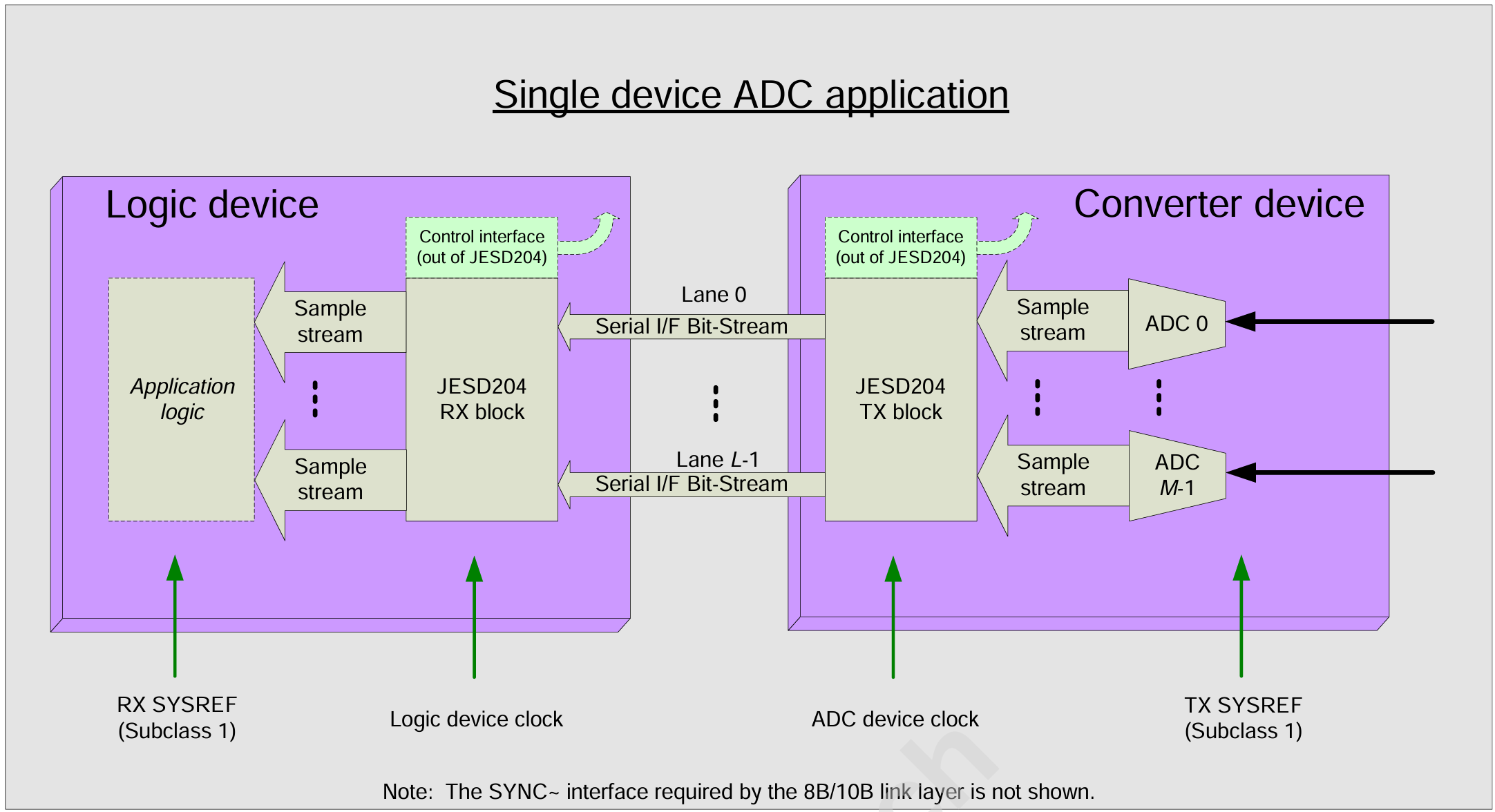
Figure 3 illustrates a typical implementation of the interface as it applies to a single ADC device communicating with a single logic device. With this configuration, a single package contains one or more ADCs. As described earlier, the converters' output data is aggregated by the JESD204 TX block and is sent across one or more lanes to the receiving logic device.
The logic device de-serializes the data in the JESD204 RX block. If multiple lanes are involved, the logic device RX block is also responsible for ensuring alignment of the data streams being sent to the application logic.
In subclass 1, the zero-to-one transitions on the signals marked as TX SYSREF and RX SYSREF are sampled by the ADC Device clock and the Logic Device clock respectively, thereby synchronizing the LMFC/LEMC phase inside each of the devices.
5.3 Single-device DAC application
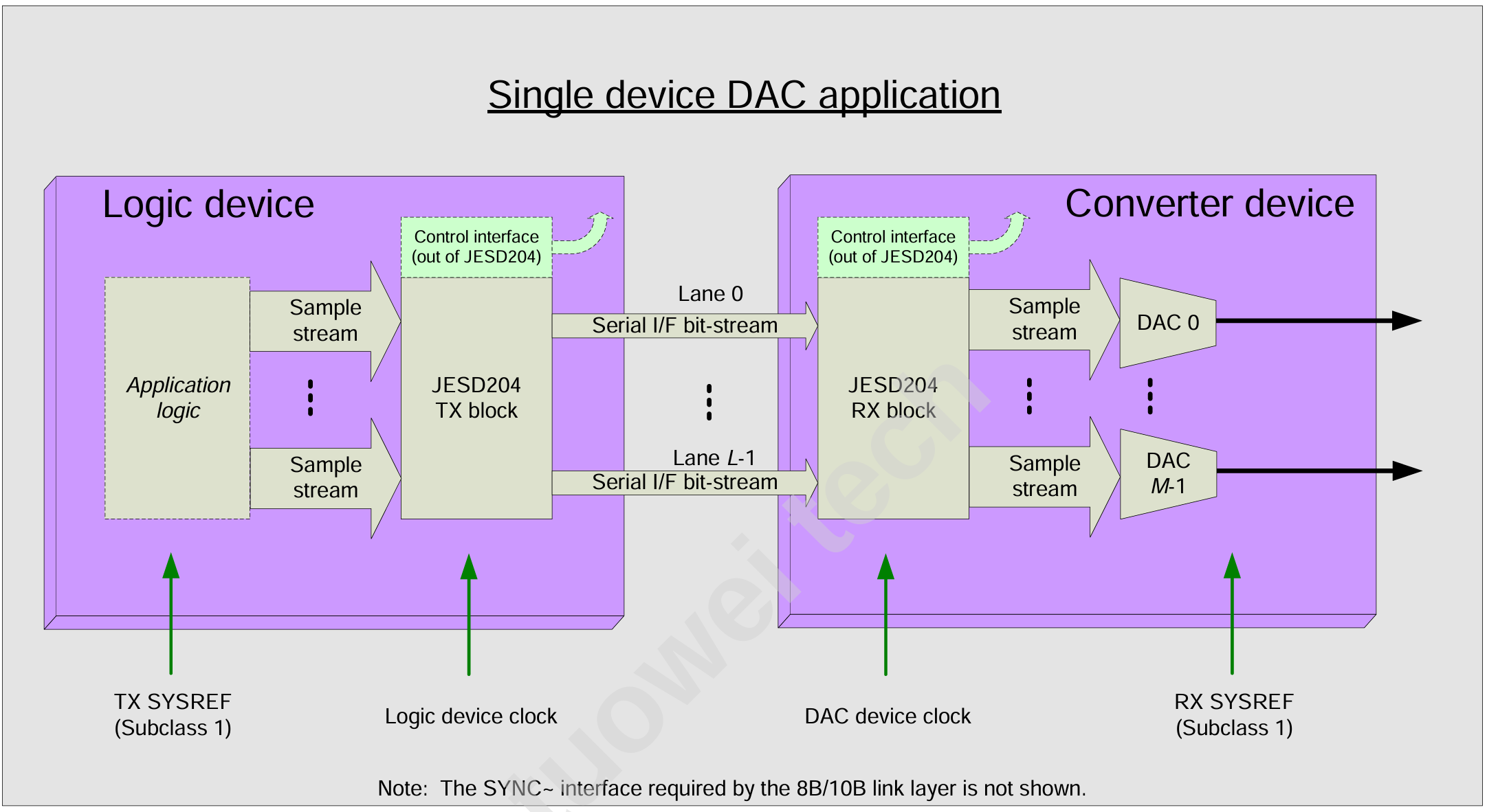
Figure 4 shows an application using multiple DACs in a single package. In this application, the logic device provides DAC samples using one or more lanes. In the DAC device's JESD204 RX block, the data is de-serialized and provided to the DACs.
In subclass 1, the zero-to-one transitions on the signals marked as TX SYSREF and RX SYSREF are sampled by the logic device clock and the DAC device clock respectively, thereby synchronizing the LMFC phase inside each of the devices.