1. Scope
This standard describes a serialized interface between data converters and logic devices. It contains normative information to enable designers to implement devices that communicate with other devices covered by this specification. Informative annexes are included to clarify and exemplify the document.
Due to the range of applications involved, the intention of this standard is to completely specify only the serial data interface and the link protocol. Certain signals common to both the interface and the function of the device, such as device clocks and control interfaces, have application-dependent requirements. The JESD204 standard does not require a specific implementation of the control interface, however a serial interface is the recommended implementation. Devices may also have application-dependent modes, such as a low power / shutdown mode that will affect the interface. In these instances, the specification merely constrains other device properties as they relate to the interface, and leaves the specific implementation up to the designer.
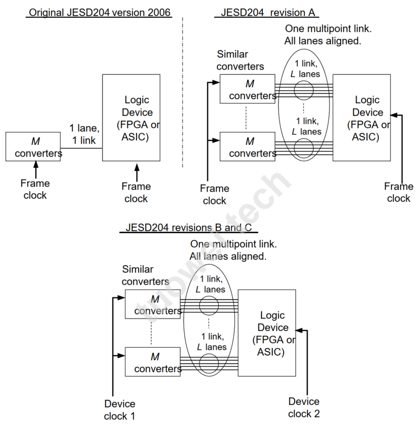
Revision A of the standard was expanded to support serial data interfaces consisting of single or multiple lanes per converter device. In addition, converter functionality (ADC or DAC) can be distributed over multiple devices:
- All parallel running devices are implemented or specified to run synchronously with each other using the same data format.
- Normally this means that they are part of the same product family.
Revision B of the standard supports the following additional functions:
- Mechanism for achieving repeatable, programmable deterministic delay across the JESD204 link.
- Support for serial data rates up to 12.5 Gbps.
- Transition from using frame clock as the main clock source to using device clock as the main clock source. Device clock frequency requirements offer much more flexibility compared to requiring a frame clock input.
Revision C of the standard now supports the following additional functions:
- Data interfaces up to 32 Gbps.
- Three link layers - 64B/66B, 64B/80B, and 8B/10B. The 8B/10B link layer is similar to the link layer defined in JESD204B.
Figure 2 compares the scope of the original JESD204 specification and its revisions. Although not illustrated in the figure, it is possible to apply multiple, independent instances of the JESD204 standard to the same device. The logic device (e.g., ASIC or FPGA) is always assumed to be a single device.