Architecture of PTA
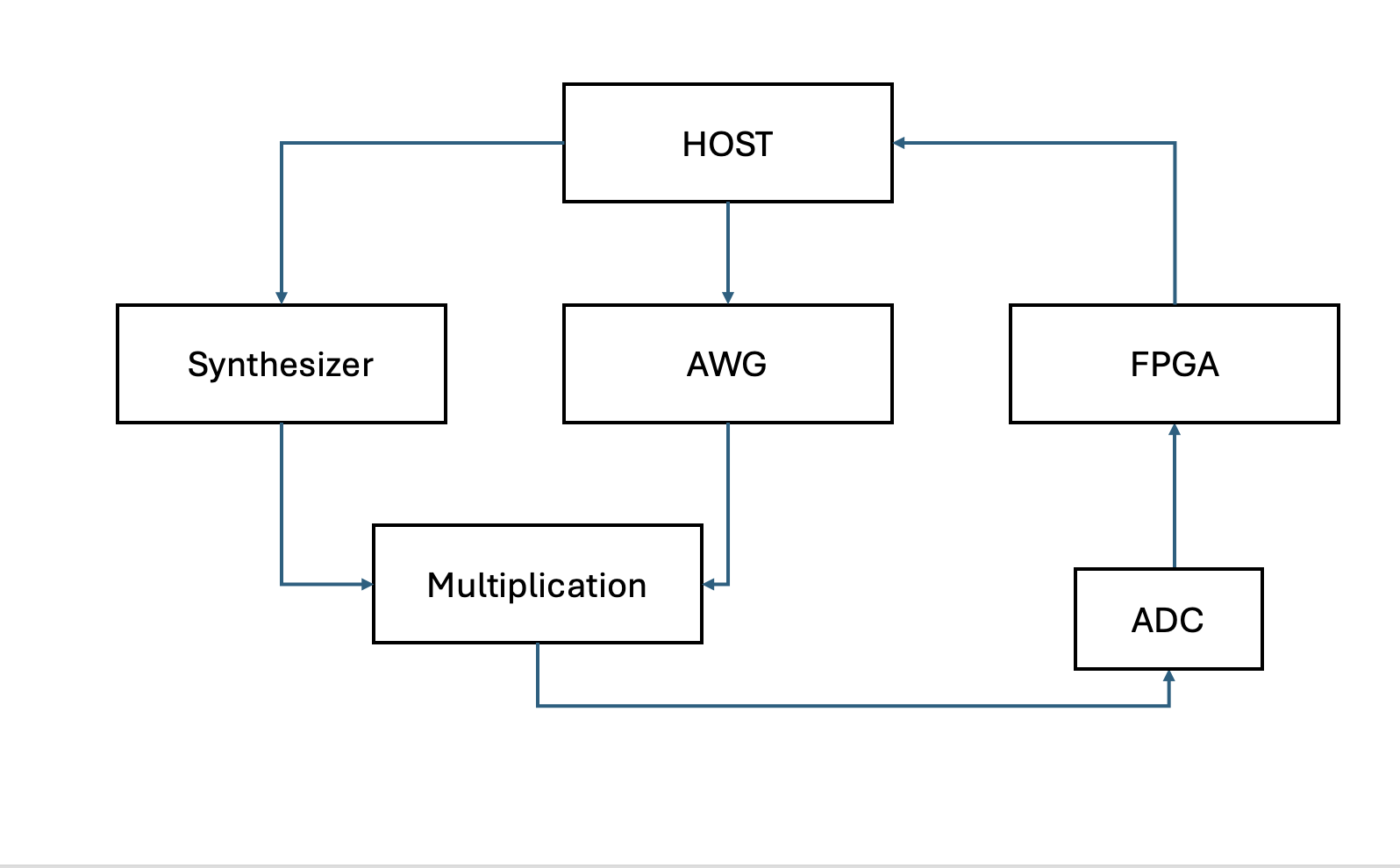
PTA sub modules
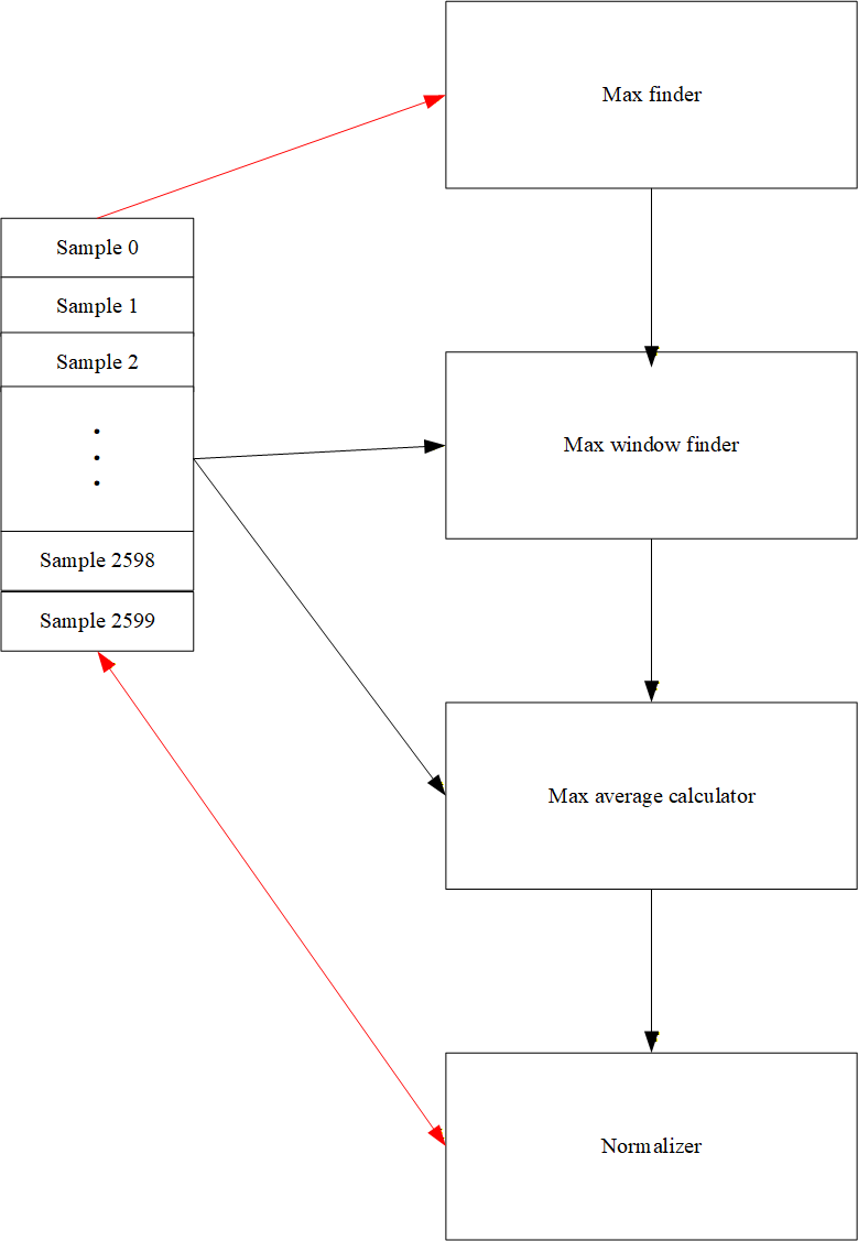
max finder
max window finder
average calculator
normalizer
ADC packet to samples
3 Design Flow Methodology
You will be provided a reference design that is customized for your application needs and targeted for a Xilinx development kit or a prototype FPGA boad. You can use it as a starting point to carry out the following (if necessary):
- Further customize the MGT transceiver block or re-map it for a different FPGA
4.2 Integrated Rx Transport Layer
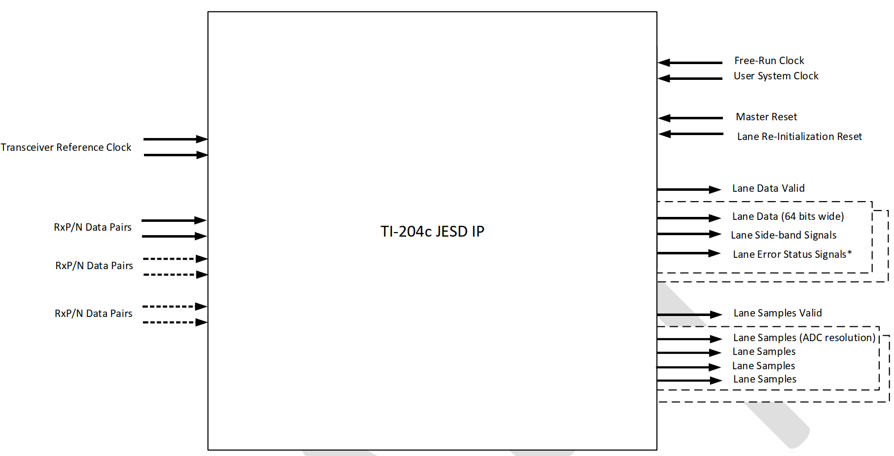
The JESD IP can also be generated with an integrated transport layer for the Rx IP that will interpret the lane data and output a desired number of samples per cycle on each lane. The FPGA designer can either use these samples for further processing, or choose to create a customized transport layer for generating the samples. The figure below illustrates an example where each lane emits 64 bit data per cycle, and the IP also has a corresponding output that exports 4 samples per cycle per lane (sorted and mapped as per the ADC resolution).
5.1 Parameter / Attribute list
ADC_RES
Default: 12
- Resolution of the ADC connected to the Rx IP
NUM_QUADS
Default: 2
- Number of Quads used in the transceiver
NUM_RX_LANES
Default: 8
- Number of Rx channels / lanes used in the transceiver
RX_LN_IDX_WIDTH
Default: 3
- Log (base2) of NUM_RX_LANES (rounded up to nearest power of 2)
- Eg: If NUM_RX_LANES = 4, RX_LN_IDX_WIDTH = 2
- Eg: If NUM_RX_LANES = 12, RX_LN_IDX_WIDTH = 4
RX_LN_DATA_WIDTH
Default: 64
- Data width of each lane of the Rx IP. Allowed values (and supported transceivers) are
- 32 : GTYP, GTY, GTHP, GTH, GTX, GTP
- 64 : GTYP, GTY, GTHP, GTH, GTX
- 128 : GTYP (64b/66b mode only)
5.2 Port List
rx_lane_data
Width: Array: NUM_RX_LANES of width RX_LN_DATA_WIDTH
Dir: OUT
Clock Domain: rx_sys_clock
- Output data buses of the Rx IP. There is one output bus per transceiver lane.
noteAll the lanes within one JESD Rx will release in a synchronized manner.
rx_lane_valid
Width: 1
Dir: OUT
Clock Domain: rx_sys_clock
- Data valid signal for the output lane data and sideband signals of the Rx IP.
- When
1, it indicates that the new data and sideband signals are valid and can be used by the downstream logic for processing. - When
0, the last valid values of the data and sideband signals will be held. These values should be discarded from downstream processing.
Therx_lane_validsignal will intermittently transition from1to0if the frequency ofrx_sys_clock(Fsysclk) is greater than the minimum value described in this table. If theFsysclkis maintained at the minimum value, the data valid will always remain1after the lanes have released.
- When
rx_lane_samples
Width: 3D array: NUM_RX_LANES arrays, each containing SAMPLES_PER_CYCLE_PER_LANE values of ADC_RES
Dir: OUT
Clock Domain: rx_sys_clock
- Output of the internal transport layer of the JESD Rx IP. This consists of the lane data, sorted into separate samples and packed into the required number of samples per cycle.
note- This is an advanced feature of the JESD Rx IP and will be provided with the customized reference design.
- The embedded transport layer may not be available for all JESD modes of the various data converters from TI.
- The embedded transport layer may add a latency between the lane data and the final output samples. If this latency is not desirable, the designer is encourage to create customized logic to map the lane data to samples.
rx_lane_samples_valid
Width: NUM_RX_LANES
Dir: OUT
Clock Domain: rx_sys_clock
- When
1, indicates that the values on therx_lane_samplesbus are valid.
noteAll the bits of the
rx_lane_samples_validoutput will transition to0to1simultaneously. If this is not the case, it indicates that samples from one (or more) of the lanes may be out of sync with the rest.
TI ADC12QJ1600-EP
JMODE 15 configuration parameters:
- Operating Mode: 12-Bit, 64B/66B, 8 Lanes
- Encoding: 64B/66B
- N: 12 bits per sample
- N’: 12 bits per sample
- CS: 0 control bits per sample
- CF: 0 control words per frame
- L: 8 lanes
- M: 8 lanes
- F: 3 octets (bytes) per frame per lane
- S: 2 samples per converter per frame
- HD: High-density format, sample split between lanes
- E: 3 multiblocks per extended multiblock
Transport Layer Data Formate
| OCTET | 0 | 1 | 2 | |||
| NIBBLE | 0 | 1 | 2 | 3 | 4 | 5 |
| D0 | A0 | A4 | ||||
| D1 | A1 | A5 | ||||
| D2 | A2 | A6 | ||||
| D3 | A3 | A7 | ||||
| D4 | B0 | B4 | ||||
| D5 | B1 | B5 | ||||
| D6 | B2 | B6 | ||||
| D7 | B3 | B7 | ||||
Celine note for JMODE 15
Data mapping with 128 bit Rx IP
- Channel A: 4 lanes
- block: 64B/66B (significant digit: 64(8 octets))
- multiblock: 32 blocks (significant digit: 32*8(octets))
- extended multiblock: 3 multiblocks (significant digit: 3328(octets))
- ADC resolution: 12 bits (significant digit: 12 bits(1.5 octets))
- sample: 3328(octets)/(1.5 octets/sample) = 512 samples
- Rx data length: 128 bits (16 octets) = 10 + 2/3 samples
- Rx Length in 512 samples: 512 samples / (10 + 2/3) samples = 48
Channel A
| OCTET | 0 | 1 | 2 | 3 | 4 | 5 | 6 | 7 | ||||||||||
| NIBBLE | 0 | 1 | 2 | 3 | 4 | 5 | 6 | 7 | 8 | 9 | 10 | 11 | 12 | 13 | 14 | 15 | ||
| D0 | A0 | A4 | A8 | A12 | A16 | A20[11:8] | ||||||||||||
| D1 | A1 | A5 | A9 | A13 | A17 | A21[11:8] | ||||||||||||
| D2 | A2 | A6 | A10 | A14 | A18 | A22[11:8] | ||||||||||||
| D3 | A3 | A7 | A11 | A15 | A19 | A23[11:8] | ||||||||||||
| OCTET | 8 | 9 | 10 | 11 | 12 | 13 | 14 | 15 | |||||||||
| NIBBLE | 16 | 17 | 18 | 19 | 20 | 21 | 22 | 23 | 24 | 25 | 26 | 27 | 28 | 29 | 30 | 31 | |
| D0 | A20[7:0] | A24 | A28 | A32 | A36 | A40[11:4] | |||||||||||
| D1 | A21[7:0] | A25 | A29 | A33 | A37 | A41[11:4] | |||||||||||
| D2 | A22[7:0] | A26 | A30 | A34 | A38 | A42[11:4] | |||||||||||
| D3 | A23[7:0] | A27 | A31 | A35 | A39 | A43[11:4] | |||||||||||
TI ADC12QJ1600-EP
JMODE 6 configuration parameters:
- operating mode: 12-bit, 64B/66B, 6 lanes
- Encoding: 64B/66B
- N: 12 bits per sample
- N’: 12 bits per sample
- CS: 0 control bits per sample
- CF: 0 control words per frame
- L: 6 lanes
- M: 4 converters
- F: 2 octets (bytes) per frame per lane
- S: 2 samples per converter per frame
- HD: high density mode, samples split between lanes
- E: 1 multiblock per extended multiblock
Transport Layer Data Format
| OCTET | 0 | 1 | ||
|---|---|---|---|---|
| NIBBLE | 0 | 1 | 2 | 3 |
| D0 | A0[11:0] | A1[11:8] | ||
| D1 | A1[7:0] | B0[11:4] | ||
| D2 | B0[3:0] | B1[11:0] | ||
| D3 | C0[11:0] | C1[11:8] | ||
| D4 | C1[7:0] | D0[11:8] | ||
| D5 | D0[3:0] | D1[11:0] | ||
Celine note for JMODE 6
Data mapping with 128 bit Rx IP
- Channel A: 6 lanes
- block: 64B/66B (significant digit: 64(8 octets))
- multiblock: 32 blocks (significant digit: 32*8(octets))
- extended multiblock: 1 multiblock (significant digit: 32*8(octets))
- ADC resolution: 12 bits (significant digit: 12 bits(1.5 octets))
4 channels output layout
| OCTET | 0 | 1 | 2 | 3 | 4 | 5 | 6 | 7 | ||||||||
|---|---|---|---|---|---|---|---|---|---|---|---|---|---|---|---|---|
| NIBBLE | 0 | 1 | 2 | 3 | 4 | 5 | 6 | 7 | 8 | 9 | 10 | 11 | 12 | 13 | 14 | 15 |
| D0 | A0[11:0] | A1[11:8] | A2[11:0] | A3[11:8] | A4[11:0] | A5[11:8] | A6[11:0] | A7[11:8] | ||||||||
| D1 | A1[7:0] | B0[11:4] | A3[7:0] | B1[11:4] | A5[7:0] | B2[11:4] | A7[7:0] | B3[11:4] | ||||||||
| D2 | B0[3:0] | B1[11:0] | B2[3:0] | B3[11:0] | B4[3:0] | B5[11:0] | B6[3:0] | B7[11:0] | ||||||||
| D3 | C0[11:0] | C1[11:8] | C2[11:0] | C3[11:8] | C4[11:0] | C5[11:8] | C6[11:0] | C7[11:8] | ||||||||
| D4 | C1[7:0] | D0[11:8] | C3[7:0] | D1[11:8] | C5[7:0] | D2[11:8] | C7[7:0] | D3[11:8] | ||||||||
| D5 | D0[3:0] | D1[11:0] | D2[3:0] | D3[11:0] | D4[3:0] | D5[11:0] | D6[3:0] | D7[11:0] | ||||||||
| OCTET | 8 | 9 | 10 | 11 | 12 | 13 | 14 | 15 | ||||||||
|---|---|---|---|---|---|---|---|---|---|---|---|---|---|---|---|---|
| NIBBLE | 16 | 17 | 18 | 19 | 20 | 21 | 22 | 23 | 24 | 25 | 26 | 27 | 28 | 29 | 30 | 31 |
| D0 | A8[11:0] | A9[11:8] | A10[11:0] | A11[11:8] | A12[11:0] | A13[11:8] | A14[11:0] | A15[11:8] | ||||||||
| D1 | A9[7:0] | B8[11:4] | A11[7:0] | B9[11:4] | A13[7:0] | B10[11:4] | A15[7:0] | B11[11:4] | ||||||||
| D2 | B8[3:0] | B9[11:0] | B10[3:0] | B11[11:0] | B12[3:0] | B13[11:0] | B14[3:0] | B15[11:0] | ||||||||
| D3 | C8[11:0] | C9[11:8] | C10[11:0] | C11[11:8] | C12[11:0] | C13[11:8] | C14[11:0] | C15[11:8] | ||||||||
| D4 | C9[7:0] | D8[11:8] | C11[7:0] | D9[11:8] | C13[7:0] | D10[11:8] | C15[7:0] | D11[11:8] | ||||||||
| D5 | D8[3:0] | D9[11:0] | D10[3:0] | D11[11:0] | D12[3:0] | D13[11:0] | D14[3:0] | D15[11:0] | ||||||||