4.3 Physical timing
4.3.1 Device clock
The device clock is the external timing reference of each transmitter and receiver converter device in the JESD204 system. It is not mandatory that all devices share a common device clock. However, all device clocks in the system shall be phase locked to a common source, which is known as the source clock. The devices shall be able to generate and receive data at a constant rate derived from their device clock. Inside the devices, all internal clocks that influence the delay on the link shall be derived from the device clock.
The permitted relationships between the periods of the TX and RX device clock and the durations of data structures on the link depend on the JESD204 subclass as follows:
- Subclass 0: The permitted relationships between the device clock period and the duration of the frame, 8B/10B character, 64B/66B block or 64B/80B block shall be specified by the device implementer. The device implementer shall specify possible extra restrictions on the device clock period for backwards compatibility with JESD204A or JESD204B, if applicable.
- Subclass 1: The duration of the multiframe or extended multiblock shall be a whole number of device clock periods.
- Subclass 2 (8B/10B link layer only): The multiframe duration shall be a whole number of device clock periods. Additionally, the TX device clock period shall be a whole number of RX device clock periods, or the RX device clock period shall be a whole number of TX device clocks periods.
The above requirements for subclasses 1 and 2 are necessary, in order that the devices can align the LMFC or LEMC edges (see 4.3.4) to the device clock edges.
The electrical characteristics of the device clock signal are not specified in this document, because other considerations may determine these characteristics. It is expected that Low Voltage CMOS type electrical characteristics, as specified by such JEDEC standards as JESD8-5 (2.5 V) or JESD8-7 (1.8 V) would be used for this signal. Higher clock rates might demand the use of a differential signal format, such as LVPECL, LVDS or CML.
The device clock input's frequency and phase stability (jitter), however, have a direct bearing on the operation of this interface. For this reason, manufacturers shall specify the required jitter for the device clock.
Other circuitry in the transmitter or receiver device may require more restrictive jitter characteristics and may also have additional requirements such as duty cycle.
4.3.2 Link layer clock
In this standard, the link layer clock is defined as the clock that sequences the signal processing in the link layer and the parallel interface between the link layer and the physical layer. The skew budget is based on the following requirement for the duration TLLC of one link layer clock cycle:

where fb is the serial bit rate and UI is the duration of a serial bit.
JESD204 does not specify the device implementation. The device implementer may deviate from the above assumptions, but such a deviation shall not lead to a violation of the skew budget (see 4.3.8).
4.3.3 Transport layer clock
In this standard, the transport layer clock is defined as the clock that sequences the signal processing in the transport layer and the parallel interface between the transport layer and the link layer. The skew budget is based on the following requirement for the duration TTLC of one transport layer clock cycle:
For 8B/10B and 64B/80B encoding: 
For 64B/66B encoding: TTLC <= 66UI
where fb is the serial bit rate and UI is the duration of a serial bit.
JESD204 does not specify the device implementation. The device implementer may deviate from the above assumptions, but such a deviation may not lead to a violation of the skew budget (see 4.3.8).
4.3.4 Local multiframe and extended multiblock clocks (LMFC and LEMC)
The local multiframe clock (LMFC, used with 8B/10B encoded data) and the local extended multiblock clock (LEMC, used with 64B/66B and 64B/80B encoded data) are internal clocks used to align the boundaries of the multiframes or extended multiblock between lanes and - in deterministic latency devices - to an external reference (SYSREF or MULTIREF in subclass 1 and SYNC- in subclass 2). The use of an LMFC / LEMC is mandatory in subclasses 1 and 2 and optional in subclass 0.
Subclass 2 is only applicable to 8B/10B encoding.
The local multiframe / extended multiblock clocks in device subclasses 1 and 2 shall comply with the following requirements:
- The LMFC / LEMC period in all transmitter and receiver devices shall be identical.
- The LMFC / LEMC shall be derived from the device clock.
- At each side of the link, the LMFC / LEMC shall be common to all lanes of the link.
- In subclass 1 devices, there shall be a fixed or programmable offset between the rising or falling edge of the LMFC / LEMC and the device clock edge upon which the SYSREF / MULTIREF signal is detected as being active.
- Subclass 1 devices shall be able to measure the amount of device clock cycles by which the detected active edge of the SYSREF / MULTIREF signal deviates from its expected position and not to realign the LMFC / LEMC if the deviation from the expected position is less than a programmable number of device clock cycles.
If a device supports multiple JESD204 links, the above requirements are applied separately to each link.
4.3.5 SYSREF signal (device Subclass 1)
In Subclass 1 deterministic latency systems, a signal named SYSREF is distributed to all transmitter and receiver devices in the system. The purpose of SYSREF is to identify the device clock edge that shall be used to align the phase of the LMFC or LEMC.
SYSREF can be either a periodic, one-shot (strobe-type), or "gapped" periodic signal. It is an active high signal, which is sampled by the device clock. Devices shall be able to support sampling SYSREF on the device clock rising edge, but may optionally allow SYSREF to be sampled on the device clock falling edge.
For periodic or "gapped" periodic SYSREF signals, the period shall be an integer multiple of the LMFC or LEMC period. The phase of the LMFC or LEMC within a device shall be determined by the device clock sampling edge upon which the sampled SYSREF value has transitioned from "0" to "1".
It is not mandatory that a common SYSREF signal is generated to all devices in the system. However, it is required that SYSREF signals be generated to all devices in a manner that ensures a deterministic relationship between the moments when SYSREF is sampled active by all devices in the system. A timing diagram illustrating this concept (using device clock rising edge to sample SYSREF) and showing simultaneous sampling of the active SYSREF signal at both devices is shown in Figure 6.
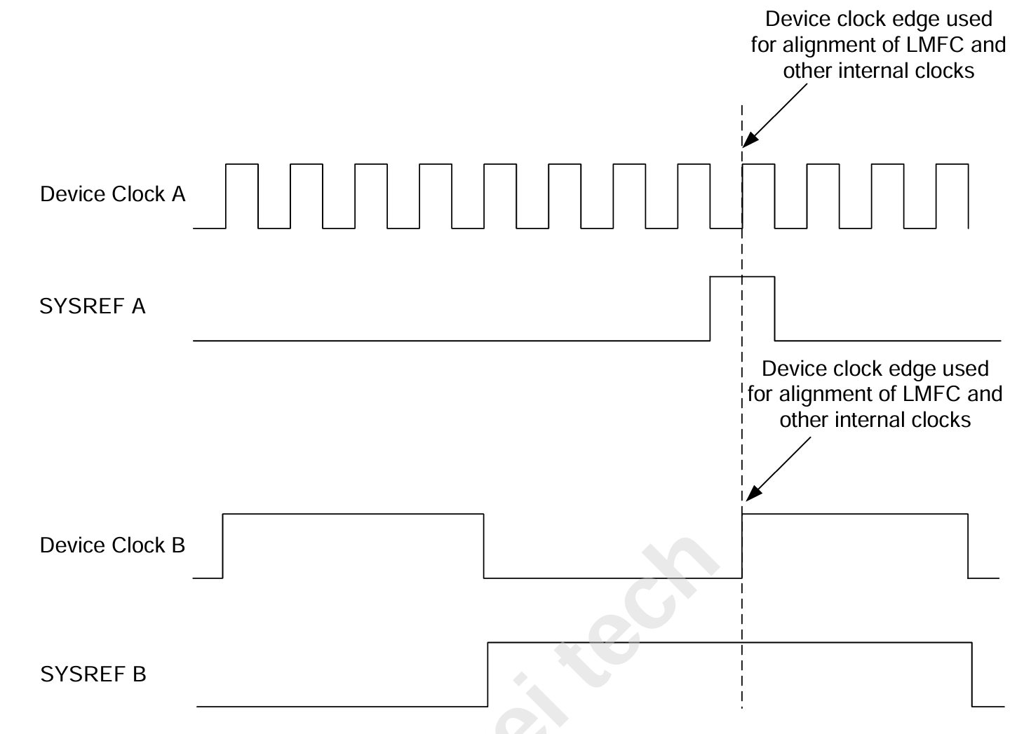
Delay uncertainty across the link is caused by the uncertainty in phase alignment between the LMFCs / LEMCs in the TX and RX devices within the system. Minimizing delay uncertainty relies on the generation of the LMFC / LEMC in both the TX and RX to be governed by events that happen at the same time instant. For Subclass-1 devices, this time instant corresponds to the device clock cycle upon which a "0" to "1" transition on SYSREF is detected. Therefore, it is recommended that the system implementer follows these guidelines for minimizing phase alignment offset between TX and RX LMFCs / LEMCs.
- The device clock and SYSREF signal to each device should be routed close to each other.
- SYSREF (source synchronous to device clock) should be distributed within the system for maximum setup/hold compliance at the device receiver.
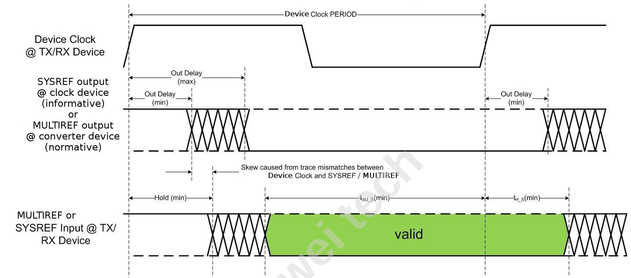
- SYSREF should ideally have the timing relationship relative to the device clock as shown in Figure 7. However, with very high speed device clocks, it may not be possible to meet SYSREF setup/hold time requirements. The resulting amount of delay uncertainty across the link can be minimized by controlling the phase of the SYSREF signal relative to the setup/hold time requirements of the device that is sampling it.
It is strongly recommended to use the same type of signal type for SYSREF and the device clock, to maintain an accurate timing relationship.
Figure 7 shows the critical timing specifications relating to the SYSREF signal. The values for these parameters are not specified here but the transmitter and receiver device specifications shall specify these values.
tSU_S(min) and tH_S(min): Setup and hold times of SYSREF with respect to device clock at the device SYSREF pin. Subclass-1 transmitter and receiver devices shall specify these parameters.
4.3.6 MULTIREF signal (device subclass 1)
In applications where lane alignment between multiple converter devices is required, but no deterministic latency is needed, the SYSREF signal may be replaced by the optional MULTIREF signal. The MULTIREF signal is fed to the SYSREF input of the converter devices. The converter devices shall use the MULTIREF signal to align their LMFCs or LEMCs, exactly in the same way as SYSREF. However, unlike SYSREF, the MULTIREF signal is generated in a converter device, not in the clock generator. For this reason, it may be more difficult to meet the setup and hold requirements relative to the device clock at the device inputs. Hence, the alignment obtained by means of the MULTIREF signal is possibly less accurate than what can be obtained by the SYSREF signal. Despite its disadvantages of no deterministic latency and possibly reduced alignment accuracy, the MULTIREF signal may be a useful option, because it simplifies the clocking architecture.
Figure 7 shows the critical timing specifications relating to the MULTIREF signal. The specification of the setup and hold times is common with the SYSREF signal. In addition, the specification of the devices that are capable of transmitting the MULTIREF signal shall specify the delay of the MULTIREF output relative to the active device clock edge. It is recommended that this delay is programmable, to facilitate compliance with the setup and hold times of the MULTIREF receiving device(s).
The timing of the MULTIREF signal is controlled by a master device. A master ADC device shall align the rising edge of the transmitted MULTIREF signal to the active edge of its LMFC or LEMC. A master DAC device shall align its LMFC or LEMC and the rising edge of the transmitted MULTIREF signal to the start of the received multiframe or extended multiblock on the latest lane. Optionally, a master device may advance the transmitted MULTIREF signal by a programmable number of device clock cycles relative to the LMFC or LEMC, to compensate the transmission delay to the slave device(s). After alignment of its LMFC to the latest lane signal, a master DAC device shall delay the received lane signals relative to the LMFC or LEMC as specified by the parameter RBD (see 4.2.1).
Slave devices accept the MULTIREF signal at their SYSREF input. A slave device shall align its LMFC or LEMC to the rising edge of the received MULTIREF signal. After alignment of its LMFC or LEMC to the received MULTIREF signal, a slave DAC device shall delay the start of the multiframe or extended multiblock of the received lane signals relative to its LMFC or LEMC as specified by the parameter RBD, see 4.2.1.
A logic device receiver connected to a multipoint ADC link that is aligned using MULTIREF, shall behave as if it were a subclass 0 receiver: the RX buffers are released at the earliest opportunity after the detection of a multiframe or extended multiblock boundary in each lane.
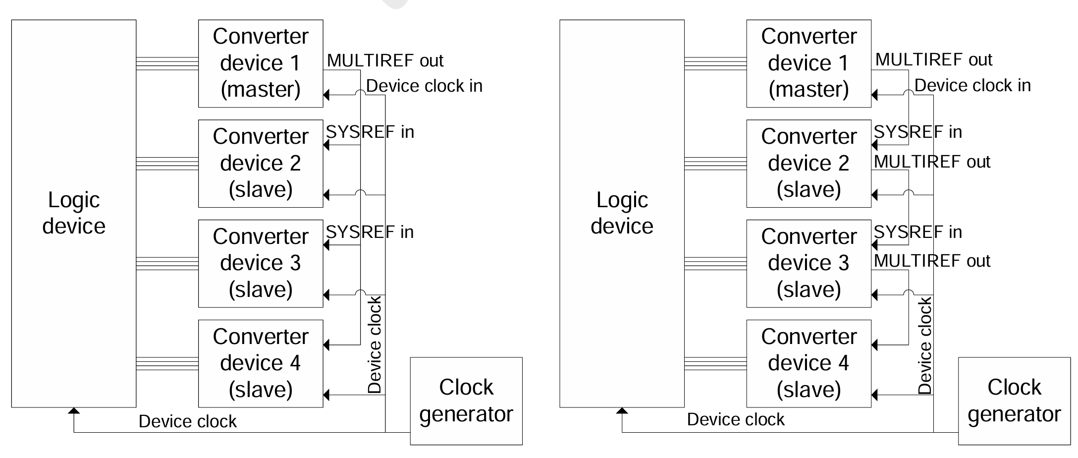
There are two kinds of MULTIREF devices possible: one-directional and repeater type. One-directional devices can either receive the MULTIREF signal or transmit it, but not simultaneously. Repeater devices receive the MULTIREF signal at their SYSREF input and forward it to a MULTIREF output. One-directional devices can be used in a multidrop topology, and repeater devices in a daisy chain topology, as illustrated in Figure 8. When using a daisy chain topology, it is recommended to use a periodic or "gapped" periodic MULTIREF signal, in order that the repeater device can regenerate the MULTIREF signal and align it to the received MULTIREF signal with essentially zero delay. A slave repeater device may optionally advance the transmitted MULTIREF signal by a programmable number of device clock cycles relative to its LMFC or LEMC, to compensate the transmission delay to the next slave device.
4.3.7 SYNC~ generation and detection clocks (8B/10B link layer)
The SYNC~ generation clock is the clock used in the RX device for generating the SYNC~ signal to the hard-wired SYNC interface (see 8.8.2). The SYNC~ detection clock is the clock used in the TX device for sampling the SYNC~ signal from the hard-wired SYNC interface (see 8.8.2).
In most of the expected applications, it will be possible to use the link layer clock as SYNC~ generation or detection clock. However, it may be necessary to use another clock in the following cases:
- for backward compatibility with a previous version of this standard (see Annex P);
- if the multiframe duration is not a whole number of link layer clock periods;
- to provide a sufficiently fine detection resolution in a subclass-2 TX (see 8.5.3.4).
In device subclasses 1 and 2, the SYNC~ generation and detection clocks shall operate at a harmonic of the LMFC and be phase aligned to the LMFC.
The duration TSYNCCLK of one cycle of the SYNC~ generation or detection clock shall comply to the following requirements:
For subclass 1 devices: TSYNCCLK <= 80UI
For subclass 2 devices: 
where fb is the serial bit rate and UI is the duration of a serial bit.
The above requirements ensure that the TX device can distinguish a synchronization request from an error report (see 8.8.2). The requirement for subclass 2 devices ensures in addition that the SYNC~ generation and detection clocks will not be slower than the slowest expected link layer clock, so that the skew budget can be based on the assumptions for the link layer clock.
4.3.8 Skew and latency variation budget
Skew is introduced at various places in the link(s) and within the clock distribution circuit. The implementation of the system shall be such that certain amounts of skew can be tolerated without affecting system performance. In JESD204 this means that all data generated simultaneously at the TX side will be aligned to the same clock edge at the RX side. Deterministic latency requires in addition alignment to a predictable device clock edge.
Skew compares signals at either the receiving or the transmitting side of the link, not signals at opposite sides of the link.
The total skew budget can be broken down into the following parts:
a) Transmission skew: the skew contribution due to the different propagation delays in the transmission medium for different lanes. b) Processing skew: the skew contribution due to the different signal processing delays inside the devices for different lanes. Processing skew includes the effects of both physical delays and clock domain crossings. c) Timing reference skew: the skew contribution due to the different arrival times of timing reference signals at the converter devices connected to a multipoint link. In JESD204, these timing reference signals are the device clock and, depending on the type of the link layer and the device subclass, SYSREF (optionally MULTIREF) and SYNC~.
Wander is not counted in the skew value, see OIF-CEI-03.1 subclause 1.6 [13].
Transmission skew and processing skew are generally larger for multipoint links than for single links. Inside a link, the lane lengths in the transmission medium are usually matched. Between links, there may be a significant difference in lane lengths. Inside the devices, the input or output pins belonging to a single link are usually situated next to each other. The pins of different links of a multipoint link may be situated at different edges of the device package, which could lead to a significant difference in propagation delays inside large (logic) devices. Although this difference in propagation delay can be compensated by extra buffering in the shorter paths, the physical distance between the links will cause increased sensitivity to PVT and clock skew in the device. Between converter devices, the delays caused by e.g., clock boundary transitions can be different. The skew budgets have therefore an allowance for extra skew on multipoint links. This allowance is modelled by the items inter-link transmission skew and inter-link processing skew.
All deterministic latency devices are required to support multipoint links. The system implementer will generally adjust the same deterministic latency on all links of a multipoint link. Therefore, the receive buffer on the fastest lane in the system shall be able to compensate for the extra delay on the slowest lane. Hence, the receive buffer of a deterministic latency device shall be dimensioned for the maximum skew on the multipoint link. Also, the system implementer will generally adjust the same deterministic latency on each board. Even if there is only a single link, this link could be "fast" on one board and "slow" on another board. Hence, also in case of a single link, the receive buffer shall be dimensioned for the maximum skew on the multipoint link.
Multipoint links can use one of the alignment reference signals: SYNC~, SYSREF or MULTIREF, to align lanes across devices, depending on the type of link layer and the device subclass. In general, the lanes are aligned to the active device clock edge on which a low-to-high transition of the alignment reference signal is detected. If the alignment reference signal would have a fixed timing relationship to the device clock at the device pins and setup and hold times were always met, the total effect of the timing reference skew on the timing misalignment between the lanes would thus be equal to the skew of the alignment reference signals. However, because the above conditions are not always met, the total effect may be larger by one RX or TX device clock cycle, or the sum of one RX and one TX device clock cycle, depending on which side(s) of the link the timing reference signals are received.
The skew budgets assume pessimistically that all items add up with the same sign. However, by prudent design of the layout on the board and in the devices, the system or device designer may be able to ensure that certain skew items add with opposite sign and the total skew is less than assumed in the below budgets.
The items in the skew budget are illustrated in Figure 9 and Figure 10.
[FIGURE 9 - Illustration of skew items in configuration with multiple ADC devices]
text
[FIGURE 10 - Illustration of skew items in configuration with multiple DAC devices]
text
The skew is specified at the following skew points, as shown in Figure 11 and Figure 12:
- SP0 = the input of the TX transport layer = reference point for deterministic latency.
- SP1 = the input of the TX link layer.
- SP2 = the output of the TX physical layer / input of the transmission medium.
- SP3 = the output of the transmission medium / input to the RX physical layer.
- SP4 = the output of the RX link layer.
- SP5 = the output of the RX transport layer = reference point for deterministic latency.
[FIGURE 11 - Definition of the skew points on a multi-point ADC link]
text
[FIGURE 12 - Definition of the skew points on a multi-point DAC link]
text
The signal path contains several clock domain crossings. Annex C provides an analysis of their effects on the skew. Each clock domain crossing gives generally a delay uncertainty of one clock cycle in the receiving clock domain. In some of the clock domain crossings it may be possible to avoid this uncertainty by careful design, but in general one cannot rely on this.
In logic devices, there may be a significant distance between the transport layer - in the user logic - and the link and physical layer, which are IP blocks by the logic device vendor situated at the periphery of the device. Therefore, in logic devices the inter-link processing skew is mainly caused by the delay differences in the connection between the transport layer and the link layers.
In converter devices, assuming a single link per device, each link is in principle identical and each device operates essentially at the same temperature and supply voltage. Therefore, if the skew budget for a single converter device allows already the maximum possible skew of one receiving clock cycle per clock domain crossing, no extra margin for inter-link processing skew is necessary, other than for tolerances in the physical delays in the devices.
The distribution of the device clock, SYNC-, SYSREF and MULTIREF, as well as the generation of the SYSREF, are under control of the system implementer. Therefore, the skew budget allocates these skew items to the transmission medium, which is also under control of the system implementer.
Table 5 through Table 9 specify the maximum skew between lanes at the various skew points. On 64B/66B and 64B/80B links, the skew at these points is defined as the difference between the times of the earliest lane and latest lane for the bit transition in the sync header of the first block in a multiblock. On 8B/10B links, the skew is defined as the difference between the times of the earliest lane and latest lane for the bit transition between the last /K/ character to the first data bit or the start of the initial lane alignment sequence. In the transmit direction, the specification is for generated skew. In the receive direction, the specification is for the skew tolerance, such that the lanes can be aligned to the desired clock edge at the output of the JESD204 link or multipoint link. The background of the numbers in the tables is provided in Annex C.
In the tables below, the numbers (ULLC and \UTLC denote the maximum expected number of unit intervals (serial bit durations) in the link layer clock and the transport layer clock, respectively. (ULLC and (UTLC depend on the serial bit rate (f_b) as follows:
Table 5 — Skew budget for subclass 0 ADC and DAC links
| Skew point | Maximum skew* | Maximum added skew† | Added by |
|---|---|---|---|
| SP0 | 0 | 0 | Interface application-to transport layer |
| SP1 | 1.5 ns | 1.5 ns | Interface transport-to-link layer |
| SP2 | (ULLC+1) UI + 1.5 ns | (ULLC+1) UI | TX link and physical layers |
| SP3 | (ULLC+1) UI + 2.5 ns | 1 ns | Intra-link transmission skew |
| SP4 | (2·ULLC+ UTLC+1) UI + 2.5 ns | (ULLC+UTLC) UI | RX link and physical layers |
| SP5 | (2·ULLC+ UTLC+1) UI + 4 ns | 1.5 ns | Interface link-to-transport layer |
- Maximum skew is normative at skew points that are accessible by the device user, otherwise informative. † Maximum added skew is normative between skew points that are accessible by the device user, otherwise informative.
Table 6 — Skew budget for subclass 1 ADC links
| Skew point | Maximum skew*, with SYSREF | MULTIREF | Maximum added skew† | Added by |
|---|---|---|---|
| SP0 | 0 | 0 | Interface application-to transport layer |
| SP1 | 4.8 ns | 1.5 ns | Interface transport-to-link layer |
| 3.3 ns | Delay tolerance between ADC devices | ||
| SP2 | (ULLC+1) UI + 4.8 ns | (ULLC+1) UI | TX link and physical layers |
| SP3 | (ULLC+1) UI + (14.8 | 24.8) ns | 1 ns‡ | Intra-link transmission skew |
| 3 ns‡,§ | Inter-link transmission skew | ||
| 6 ns‡,§ | Device clock and SYSREF | ||
| 16 ns‡,§ | Device clock and MULTIREF | ||
| SP4 | (2·ULLC+ UTLC+1) UI + (14.8 | 24.8) ns | (ULLC+UTLC) UI | RX link and physical layers |
| SP5 | (2·ULLC+ UTLC+1) UI + (19.6 | 29.6) ns | 1.5 ns | Interface link-to-transport layer |
| 3.3 ns | Delay tolerance between links in logic device |
- Maximum skew is normative at skew points that are accessible by the device user, otherwise informative. † Maximum added skew is normative between skew points that are accessible by the device user, otherwise informative. ‡ The system implementer shall ensure that the total effect of the transmission skews, device clock and SYSREF/MULTIREF skew allocated for SP3 is no more than specified. § Either the SYSREF or the MULTIREF skew is added, depending on which signal is in use.
Table 7 — Skew budget for subclass 1 DAC links
| Skew point | Maximum skew*, with SYSREF | MULTIREF | Maximum added skew† | Added by |
|---|---|---|---|
| SP0 | 0 | 0 | Interface application-to transport layer |
| SP1 | 4.8 ns | 1.5 ns | Interface transport-to-link layer |
| 3.3 ns | Delay tolerance between links in logic device | ||
| SP2 | (ULLC+1) UI + 4.8 ns | (ULLC+1) UI | TX link and physical layers |
| SP3 | (ULLC+1) UI + (14.8 | 24.8) ns | 1 ns‡ | Intra-link transmission skew |
| 3 ns‡ | Inter-link transmission skew | ||
| 6 ns‡,§ | Device clock and SYSREF | ||
| 16 ns‡,§ | Device clock and MULTIREF | ||
| SP4 | (2·ULLC+ UTLC+1) UI + (14.8 | 24.8) ns | (ULLC+UTLC) UI | RX link and physical layers |
| SP5 | (2·ULLC+ UTLC+1) UI + (19.6 | 29.6) ns | 1.5 ns | Interface link-to-transport layer |
| 3.3 ns | Delay tolerance between DAC devices |
- Maximum skew is normative at skew points that are accessible by the device user, otherwise informative. † Maximum added skew is normative between skew points that are accessible by the device user, otherwise informative. ‡ The system implementer shall ensure that the total effect of the transmission skews, device clock and SYSREF/MULTIREF skew allocated for SP3 is no more than specified. § Either the SYSREF or the MULTIREF skew is added, depending on which signal is in use.
Table 8 — Skew budget for subclass 2 ADC links
| Skew point | Maximum skew | Maximum added skew† | Added by |
|---|---|---|---|
| SP0 | 0 | 0 | Interface application-to transport layer |
| SP1 | 4.8 ns | 1.5 ns | Interface transport-to-link layer |
| 3.3 ns | Delay tolerance between ADC devices | ||
| SP2 | (ULLC+1) UI + 4.8 ns | (ULLC+1) UI | TX link and physical layers |
| SP3 | (2·ULLC+1) UI + 14.8 ns | 1 ns* | Intra-link transmission skew |
| 3 ns* | Inter-link transmission skew | ||
| ULLC UI + 6 ns* | Device clock and SYNC~ | ||
| SP4 | (3·ULLC+ UTLC+1) UI + 14.8 ns | (ULLC+UTLC) UI | RX link and physical layers |
| SP5 | (3·ULLC+ UTLC+1) UI + 19.6 ns | 1.5 ns | Interface link-to-transport layer |
| 3.3 ns | Delay tolerance between links in logic device |
- Maximum skew is normative at skew points that are accessible by the device user, otherwise informative. † Maximum added skew is normative between skew points that are accessible by the device user, otherwise informative. ‡ The system implementer shall ensure that the total effect of the transmission skews, device clock and SYNC~ skew allocated for SP3 is no more than specified.
Table 9 — Skew budget for subclass 2 DAC links
| Skew point | Maximum skew | Maximum added skew† | Added by |
|---|---|---|---|
| SP0 | 0 | 0 | Interface application-to transport layer |
| SP1 | 4.8 ns | 1.5 ns | Interface transport-to-link layer |
| 3.3 ns | Delay tolerance between links in logic device | ||
| SP2 | (ULLC+1) UI + 4.8 ns | (ULLC+1) UI | TX link and physical layers |
| SP3 | (2·ULLC+1) UI + 14.8 ns | 1‡ | Intra-link transmission skew |
| 3‡ | Inter-link transmission skew | ||
| ULLC UI + 6 ns‡ | Device clock and SYNC~ | ||
| SP4 | (3·ULLC+ UTLC+1) UI + 14.8 ns | (ULLC+UTLC) UI | RX link and physical layers |
| SP5 | (3·ULLC+ UTLC+1) UI + 19.6 ns | 1.5 ns | Interface link-to-transport layer |
| 3.3 ns | Delay tolerance between DAC devices |
- Maximum skew is normative at skew points that are accessible by the device user, otherwise informative. † Maximum added skew is normative between skew points that are accessible by the device user, otherwise informative. ‡ The system implementer shall ensure that the total effect of the transmission skews, device clock and SYNC~ skew allocated for SP3 is no more than specified.
Table 10 and Table 11 specify the maximum skew variation between lanes. Skew variation is defined as the change in skew between any two lanes over the entire time that the link is in operation, excluding the effects of re-initialization. Each layer shall produce no more skew variation than specified and shall maintain alignment of the data to the chosen clock edge when the skew variation at its input is within the specification. The background of the numbers in the tables is provided in Annex C.
Table 10 — Maximum skew variation for subclass 0 ADC and DAC links
| Skew point | Maximum skew variation* (ns) | Maximum added skew variation† (ns) | Added by |
|---|---|---|---|
| SP0 | 0 | 0 | Interface application-to transport layer |
| SP1 | 0.2 | 0.2 | Interface transport-to-link layer |
| SP2 | 0.6 | 0.4 | TX link and physical layers |
| SP3 | 0.8 | 0.2 | Transmission skew |
| SP4 | 1.2 | 0.4 | RX link and physical layers |
| SP5 | 1.4 | 0.2 | Interface link-to-transport layer |
- Maximum skew variation is normative at skew points that are accessible by the device user, otherwise informative. † Maximum added skew variation is normative between skew points that are accessible by the device user, otherwise informative.
Table 11 — Maximum skew variation for subclass 1 and 2 links
| Skew point | Maximum skew variation* (ns) | Maximum added skew variation† (ns) | Added by |
|---|---|---|---|
| SP0 | 0 | 0 | Interface application-to transport layer |
| SP1 | 0.2 | 0.2 | Interface transport-to-link layer |
| SP2 | 0.6 | 0.4 | TX link and physical layers |
| SP3 | 3.2 | 0.2 | Transmission skew |
| 2.4‡ | Device clock and SYSREF / MULTIREF / SYNC~ | ||
| SP4 | 3.6 | 0.4 | RX link and physical layers |
| SP5 | 3.8 | 0.2 | Interface link-to-transport layer |
- Maximum skew variation is normative at skew points that are accessible by the device user, otherwise informative. † Maximum added skew variation is normative between skew points that are accessible by the device user, otherwise informative. ‡ Tolerance of the maximum specified skew variation of device clock and SYSREF / MULTIREF / SYNC~ may require the capability of the RX and TX devices not to re-align the LEMC / LMFC if the detected SYSREF / MULTIREF / SYNC~ edge deviates no more than a specified amount from its expected position.