6.3 Feature Description
6.3.1 Analog Input
The analog input of the device has an internal buffer to enable high input bandwidth and to isolate sampling capacitor glitch noise from the input circuit. The analog input must be driven differentially because operation with a single- ended signal results in degraded performance. Both AC-coupling and DC-coupling of the analog input is supported. The analog input is designed for an input common-mode voltage VCMI of 1.1V which is terminated internally through single-ended, 50-Ω resistors to the VA11 supply on each input pin. DC-coupled input signals must have a common-mode voltage that meets the device input common-mode requirements specified as VCMI in the Recommended Operating Conditions table. The device includes internal analog input protection to protect the ADC input during over-range input conditions; see the Analog Input Protection section. Figure 6-2 provides a simplified analog input model.

6.3.1.1 Analog Input Protection
The analog input is protected against overdrive conditions by internal clamping diodes that are capable of sourcing or sinking input currents during over-range conditions, see the voltage and current limits in the Absolute Maximum Ratings table. The over-range protection is also defined for a peak RF input power in the Absolute Maximum Ratings table, which is frequency independent. Operation above the maximum conditions listed in the Recommended Operating Conditions table results in an increase in failure-in-time (FIT) rate, so the system must correct the overdrive condition as quickly as possible. Figure 6-2 shows the analog input protection diodes.
6.3.1.2 Full-Scale Voltage VFS Adjustment
Input full- scale voltage VFS adjustment is available, in fine increments, through FS_RANGE. All inputs are set to the same full-scale voltage setting. The available adjustment range is specified in the DC Specifications table. Larger full-scale voltages improve SNR and noise floor (in dBFS/Hz) performance.
6.3.1.3 Analog Input Offset Adjust
The input offset voltage for each analog input of the quad channel device can be adjusted through the OFSxy registers, where x represents the ADC core (0, 1, 2, 3, 4 or 5) and y represents the analog input for ADC core 2 (A or B) and core 3 (C or D). The y parameter is omitted for ADC core 0, 1, 4 and 5 since these cores always sample the same analog input. The y parameter is omitted for ADC core 0 and 1 since these cores always sample the same analog input. For the single channel device, x represents the ADC core (0 or 2) and the y parameter is omitted for ADC core 0 since this core always samples the same analog input. The adjustment range is approximately 33 mV to -33 mV differential. See the Calibration Modes and Trimming section for more information.
6.3.1.4 ADC Core
The device consists of a total of six ADC cores. The cores are swapped on- the- fly for calibration as required by the operating mode. This section highlights the theory and key features of the ADC cores.
6.3.1.4.1 ADC Theory of Operation
The differential voltages at the analog inputs are captured by the rising edge of CLK±. After capturing the input signal the ADC converts the analog voltage to a digital value by comparing the voltage to the internal reference voltage. If the voltage on the negative input (that is, INA–) is higher than the voltage on the positive input (that is, INA+) then the digital output is a negative 2's complement value. If the voltage on the positive input is higher than the voltage on the negative input then the digital output is a positive 2's complement value. Equation 1 can calculate the differential voltage at the input pins from the digital output.

Where:
Codeis the signed decimal output code (for example, -2048 to +2047)Nis the ADC resolutionV<sub>FS</sub>is the full-scale input voltage of the ADC as specified in the DC Specifications table, including any adjustment performed by programmingFS_RANGE
6.3.1.4.2 ADC Core Calibration
ADC core calibration is required to optimize the analog performance of the ADC cores. Calibration must be repeated when operating conditions change significantly, namely temperature, in order to maintain optimal performance. The device has a built- in calibration routine that can be run as a foreground operation or a background operation. Foreground operation requires ADC downtime, where the ADC is no longer sampling the input signal, to complete the process. Background calibration can be used to overcome this limitation and allow constant operation of the ADC. See the Calibration Modes and Trimming section for detailed information on each mode.
6.3.1.4.3 Analog Reference Voltage
The reference voltage for the device is derived from an internal band-gap reference. A buffered version of the reference voltage is available at the BG pin for user convenience. This output has an output-current capability of ±100μA. The BG output must be buffered if more current is required. No provision exists for the use of an external reference voltage, but the full-scale input voltage can be adjusted through the full-scale-range register settings. Note that the VA11 supply voltage should be used to set the output common-mode voltage of a front-end fully-differential amplifier and the BG output should not be used for this purpose.
6.3.1.4.4 ADC Over-range Detection
For the system gain management to have a quick response time, a low-latency configurable over-range function is included. The over-range function works by monitoring the converted 12-bit samples at the ADC to quickly detect if the ADC is near saturation or already in an over-range condition. The absolute value of the upper 8 bits of the ADC data are checked against a programmable threshold, OVR_TH. The threshold programmed into OVR_TH is used for all analog inputs. Table 6-1 lists how an ADC sample is converted to an absolute value for a comparison of the thresholds.
| ADC SAMPLE (Offset Binary) | ADC SAMPLE (2's Complement) | ABSOLUTE VALUE | UPPER 8 BITS USED FOR COMPARISON |
|---|---|---|---|
| 1111 1111 1111 (4095) | 0111 1111 1111 (+2047) | 111 1111 1111 (2047) | 1111 1111 (255) |
| 1111 1111 0000 (4080) | 0111 1111 0000 (+2032) | 111 1111 0000 (2032) | 1111 1110 (254) |
| 1000 0000 0000 (2048) | 0000 0000 0000 (0) | 000 0000 0000 (0) | 0000 0000 (0) |
| 0000 0001 0000 (16) | 1000 0001 0000 (−2032) | 111 1111 0000 (2032) | 1111 1110 (254) |
| 0000 0000 0000 (0) | 1000 0000 0000 (−2048) | 111 1111 1111 (2047) | 1111 1111 (255) |
Over-range detection is enabled by setting OVR_EN to 1. If the upper 8 bits of the absolute value equal or exceed the OVR_TH threshold during the monitoring period, then the over-range bit associated with the over-ranged ADC channel is set to 1, otherwise the over-range bit is 0. For the Quad channel device, the over-range status can be monitored on the ORA, ORB, ORC or ORD output pins for ADC channels A, B, C and D, respectively. OVR_N can be used to set the output pulse duration from the last over-range event. Table 6-2 lists the over-range pulse lengths for the various OVR_N settings.
| OVR_N | over-range PULSE LENGTH SINCE LAST over-range EVENT (DEVCLK Cycles) |
|---|---|
| 0 | 8 |
| 1 | 16 |
| 2 | 32 |
| 3 | 64 |
| 4 | 128 |
| 5 | 256 |
| 6 | 512 |
| 7 | 1024 |
Typically, the OVR_TH threshold is set near the 8-bit full-scale value (228 for example). When the threshold is triggered, a typical system turns down the system gain to avoid clipping. The downstream logic device then monitors the output samples to determine when the over-range condition no longer exists and then increases the system gain as desired.
6.3.1.4.5 Code Error Rate (CER)
ADC cores can generate bit errors within a sample, often called code errors (CER) or referred to as sparkle codes, resulting from meta-stability caused by non-ideal comparator limitations. The device uses a unique ADC architecture that inherently allows significant code error rate improvements from traditional pipelined flash or successive approximation register (SAR) ADCs. The code error rate of the device is multiple orders of magnitude better than what can be achieved in alternative architectures at equivalent sampling rates providing significant signal reliability improvements.
6.3.2 Temperature Monitoring Diode
A built-in thermal monitoring diode is made available on the TDIODE+ and TDIODE– pins. This diode facilitates temperature monitoring and characterization of the device in higher ambient temperature environments. Although the on-chip diode is not highly characterized, the diode can be used effectively by performing a baseline measurement (offset) at a known ambient or board temperature and creating a linear equation with the diode voltage slope provided in the DC Specifications table. Perform offset measurement with the device unpowered or with the PD pin asserted to minimize device self-heating. Only assert the PD pin long enough to take the offset measurement. Recommended monitoring devices include the LM95233 device and similar remote-diode temperature monitoring products from Texas Instruments.
6.3.3 Timestamp
The TMSTP+ and TMSTP– differential input can be used as a time-stamp input to mark a specific sample based on the timing of an external trigger event relative to the sampled signal. The TMSTP± input is retimed to the internal sampling clock and can be repeated out of the TRIGOUT± output to trigger external devices, such as a laser driver, when TRIGOUT_EN is set to 1 to enable the TRIGOUT± output and TRIGOUT_MODE is set to 3. The TMSTP± input can also be sent over the JESD204C interface to mark a specific ADC sample. TIME_STAMP_EN must be set in order to output the timestamp data. When enabled, the timestamp signal is sent over the JESD204C interface in place of the LSB of the JESD204C mode sample size (based on N' parameter in Table 6-15). For example, in JMODE 0 the JESD204C sample size (N') is 12 and therefore the timestamp information is sent at LSB ([0]) bit location and the 12-bit sample (truncated to 11-bits) is sent in the [11:1] bit location. The input applied to TMSTP± can be asynchronous to the ADC sampling clock and is sampled at approximately the same time as the analog input. Effectively, the TMSTP± input acts as a 1-bit ADC sampled in parallel with the ADC cores and both have matched latency through the device. The TMSTP± input must be enabled (TMSTP_RECV_EN) to use the timestamp feature.
6.3.4 Clocking
The input to the clocking subsystem of the device includes two clock inputs (CLK± and SE_CLK) and a synchronization signal (SYSREF±). An internal phase- locked loop (PLL) and voltage- controlled oscillator (VCO) can optionally be used to generate the ADC sampling clock from a low frequency reference by setting the PLL_EN pin high. The sampling clock PLL is called the converter PLL (C- PLL). The C- PLL reference can be provided to either the CLK± differential input or the SE_CLK single- ended input. The single- ended C- PLL reference input is selected by setting the PLLREF_SE pin high. For highest performance, the internal C- PLL can be bypassed and the sampling clock provided directly to the CLK± input when PLL_EN and PLLREF_SE are held low. Note that SE_CLK cannot be used if the C- PLL is disabled. The C- PLL reference clock can be sent to either an FPGA or ASIC or to an adjacent device through the PLLREFO± LVDS output when the PLL is enabled. Two additional copies or divided copies of PLLREFO can be output on ORC and ORD when enabled through the CLKCFG[1:0] pins or through SPI. PLLREFO and the ORC and ORD clock outputs are available at device power up when the CMOS control pins (PLL_EN, CLKCFG0 and CLKCFG1) are set appropriately and if PD is held low. Toggling PD high to power down the device also powers down the clock outputs.
In addition, the SerDes block contains a PLL, called S- PLL, that generates the SerDes output clock from the ADC sampling clock. The S- PLL generated clock can be divided and output from the TRIGOUT± LVDS output and sent to an FPGA or ASIC to clock the SerDes receivers. The SYSREF signal is captured by the chosen clock input (CLK± or SE_CLK). A SYSREF Windowing block is used to measure and optimize the setup and hold timing of the SYSREF signal relative to the selected clock input. SYSREF Windowing relaxes the timing requirement of the external signals. Figure 6- 3 shows the clocking subsystem.
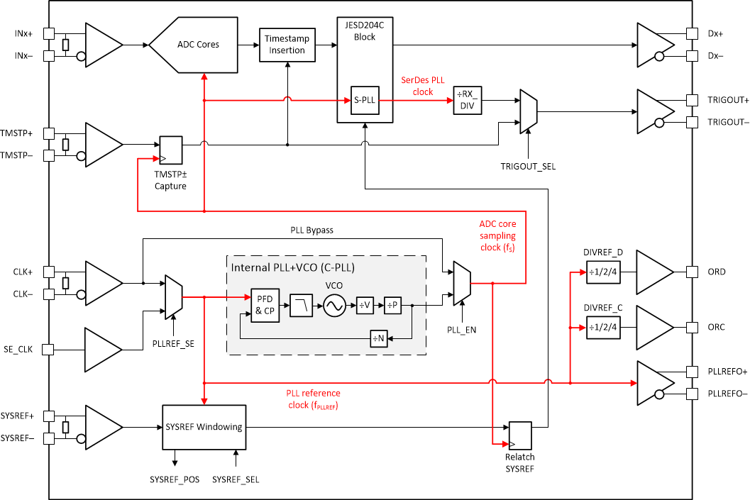
The clock generated by the C- PLL when the PLL is enabled or the clock provided to CLK± when the PLL is disabled is used as the sampling clock for the ADC core as well as the clocking for the digital processing and serializer S- PLL. Use a low- noise (low jitter) clock input, whether the PLL is enabled or disabled, to maintain high signal- to- noise ratio (SNR) within the ADC.