4 High Level Block Diagram
4.1 Basic Block Diagram and Port List
Figure 1 below illustrates a simplified block diagram and minimal port list of the TI-204c JESD FPGA IP. While the entire IP is provided as encrypted SystemVerilog code, the transceiver instantiation module (marked in green) is left as regular source code. This is to enable the designer to make further customizations to the transceiver (if necessary).
The ports marked in red are the typical board level connections for the transceiver and consist of the following:
- Transceiver Reference Clock (one differential pair per clock buffer)
- Transceiver Data Rx/Tx Pins (one differential pair per lane)
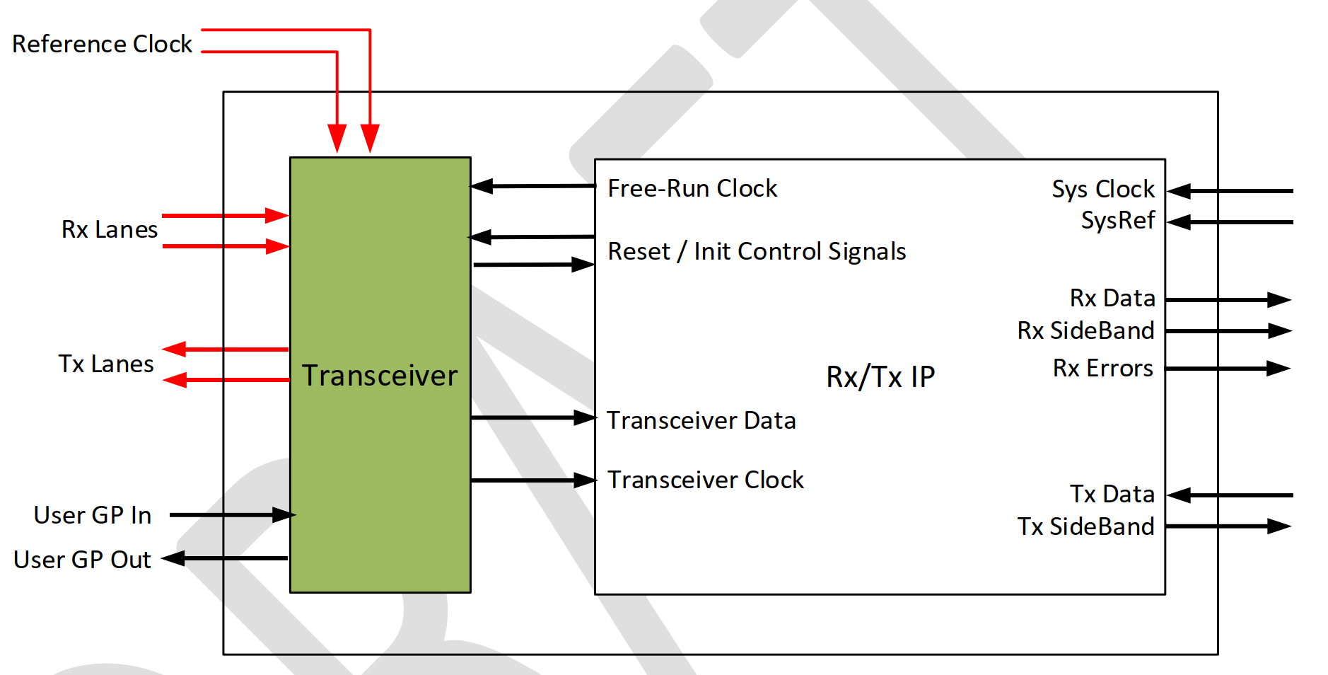
The ports on the right are connected to and controlled by the application logic in the FPGA. These fall into the following general categories:
- Clocks: These are the basic clocks needed to operate the IP
- Resets: These are the reset controls for initializing and IP and subsequently the JESD link
- Lane Specific signals: These form the actual data payload that is received over the JESD link
- Lane Rx/Tx Data : this is generated in 32/64/128 bit packets
- Sideband signals : These indicate frame / multiframe / multi-block and extended multi-block boundaries
- Error signals : These reflect lane specific error statistics and are 8b/10b or 64b/66b protocol dependent
- User GP In / Out : These are general purpose ports provided to the designer, and can be used for customized signaling between the transceiver and the rest of the application logic. The TI204c-IP does not use these signals for any of the internal functionality.
4.2 Integrated Rx Transport Layer
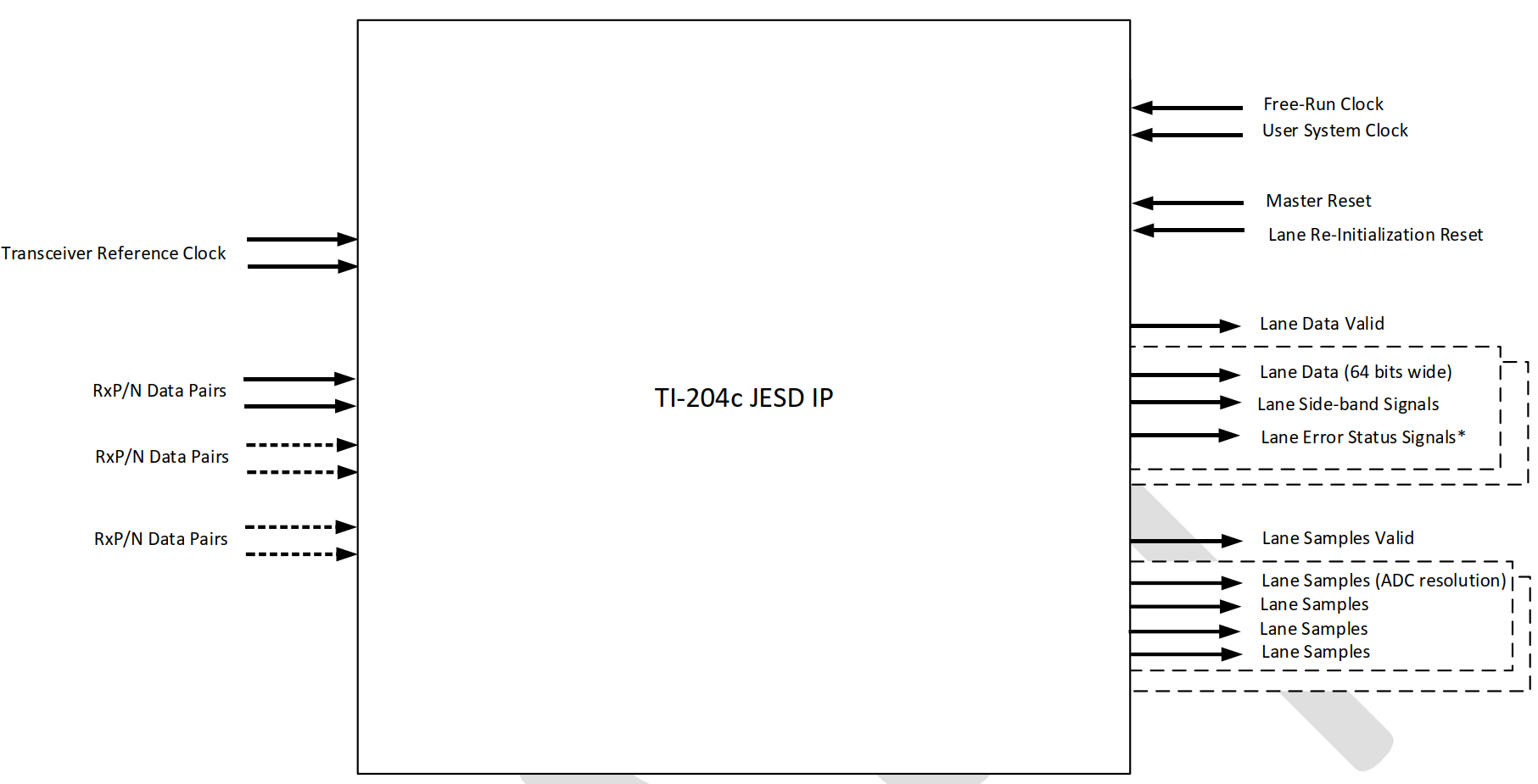
The JESD IP can also be generated with an integrated transport layer for the Rx IP that will interpret the lane data and output a desired number of samples per cycle on each lane. The FPGA designer can either use these samples for further processing, or choose to create a customized transport layer for generating the samples. The figure below illustrates an example where each lane emits 64 bit data per cycle, and the IP also has a corresponding output that exports 4 samples per cycle per lane (sorted and mapped as per the ADC resolution).
4.3 Block Diagram of the TI-204c IP
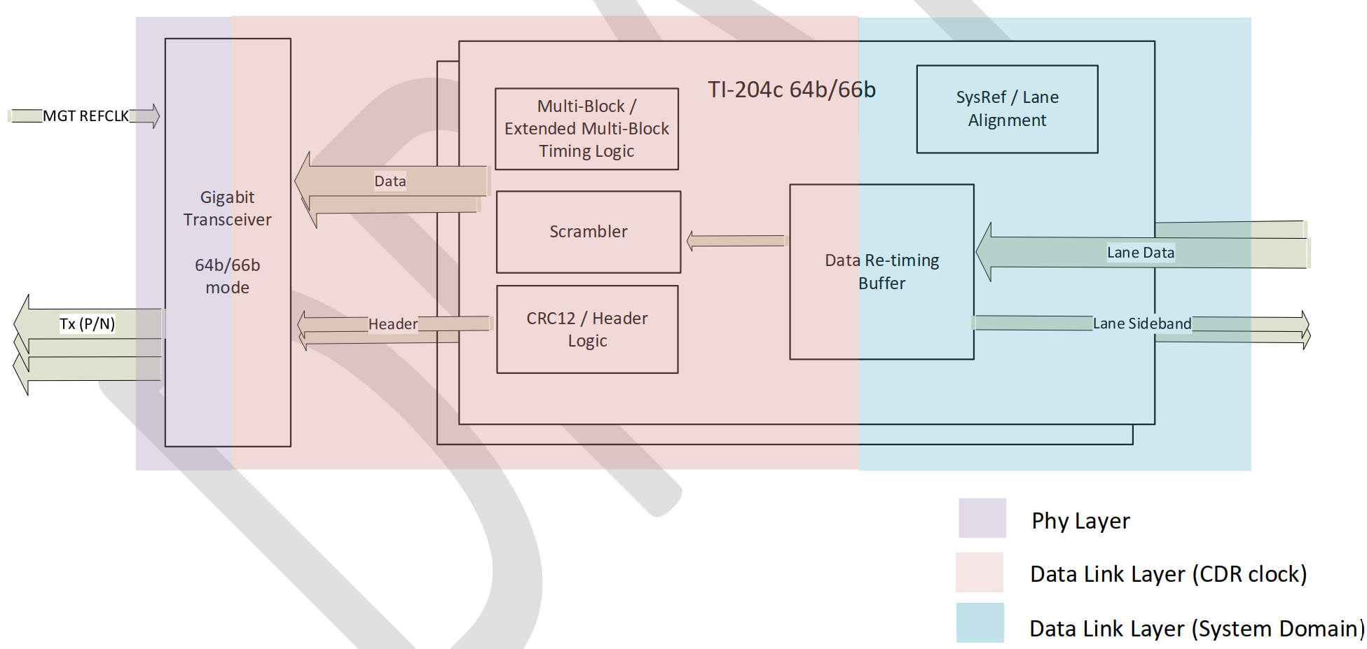
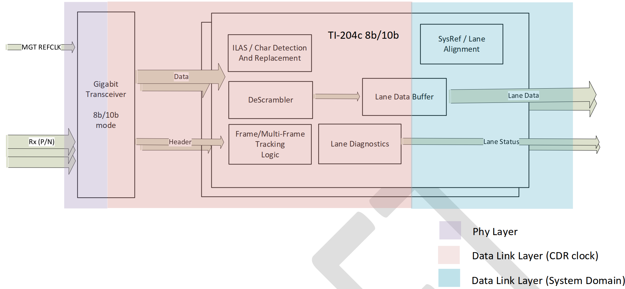
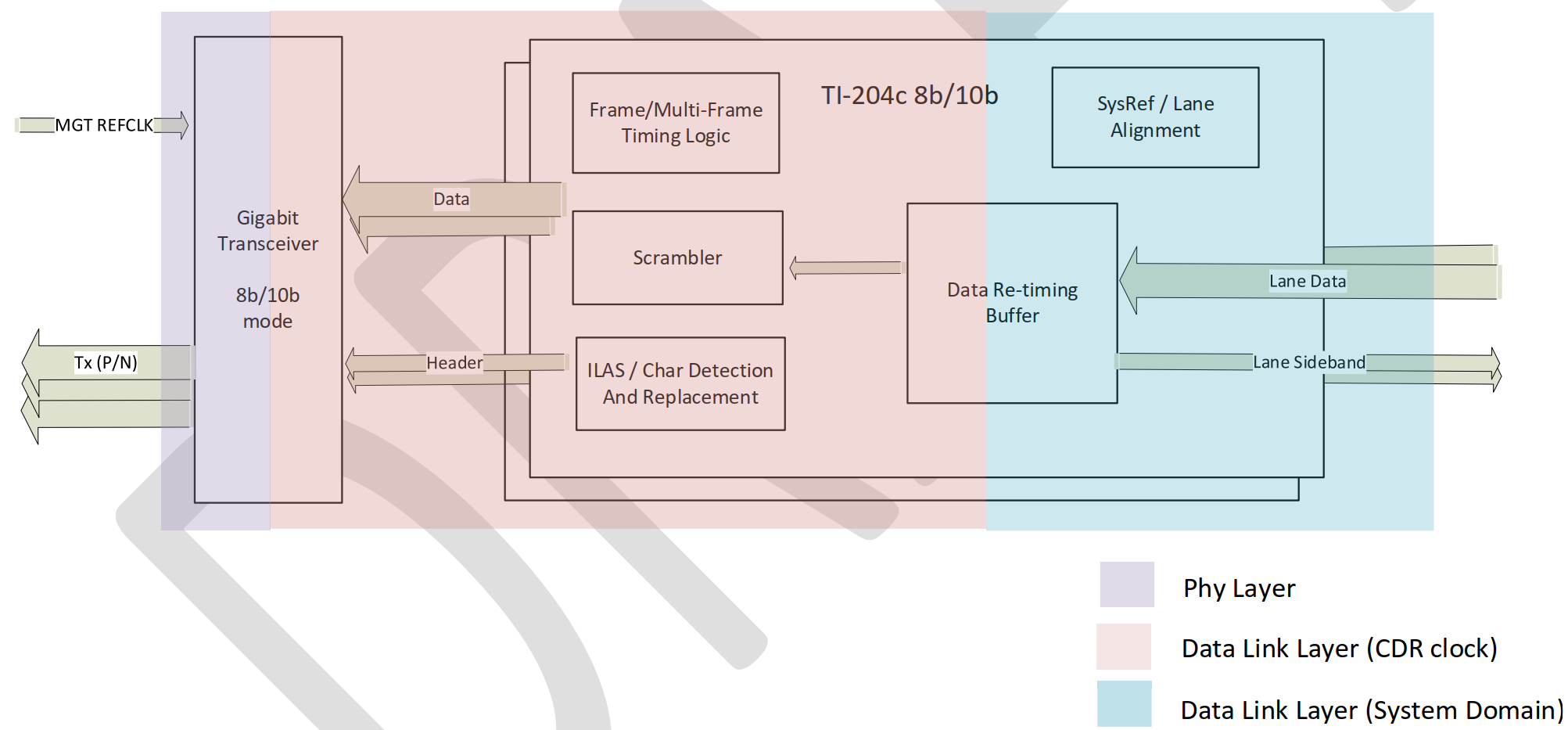
The following sub-sections illustrates the block diagram of the IP when configured in its various modes (Rx/Tx) with the two protocols (8b/10b and 64b/66b). The three colors indicate three independent clock domains:
- The domain in purple is the SERDES line rate domain and is restricted to being located within the transceiver.
- The domain in red/orange is where the primary protocol related data handling and error checking is carried out
- The domain in blue is the clock that interacts with the application logic.
The JESD IP has been architected to isolate the high speed domains of the protocol from the application logic, thereby relaxing inter-domain timing constraints and improving place and route runtimes for the tool.
4.3.1 Rx IP in 8b/10b mode
4.3.2 Tx IP in 8b/10b mode
4.3.3 Rx IP in 64b/66b mode
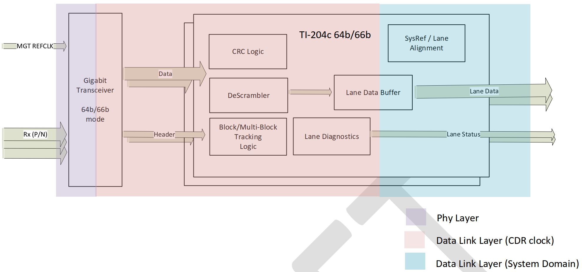
4.3.4 Tx IP in 64b/66b mode