Clocking
!! Important: It is strongly recommended that you use one of the clocking schemes presented in this section. Use of alternative clocking schemes might lead to design failure.
The JESD204C specification does not define specific serial line rates for any JESD204C link, but a valid range of line rates from 312.5 Mbps to 32.5 Gbps. The JESD204C core supports 8B10B linecoding at line rates from 1 Gbps to 16.375 Gbps (depending on the part and speed grade selection) and 64B66B linecoding at line rates from 1 Gbps to 32.5 Gbps (depending on the part and speed grade selection). In most instances, the serial line rate selection is governed by the specifications of the ADC/DAC device(s) to which the core is interfaced. The required operating serial line rate directly relates to the clock rate at which the core logic operates (core clock); the serial line rate also governs the selection of the reference clock required by the transceiver(s).
Core Clock 64B66B Linecoding
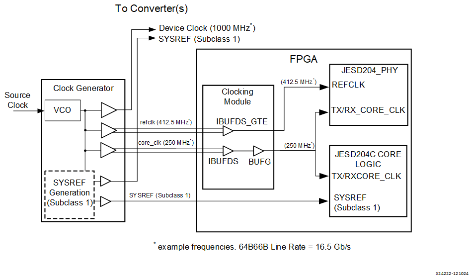
The JESD204C 64B66B core operates using a 64-bit (8-byte) datapath. The core clock frequency is always the line rate divided by 66. For example, for a serial line rate of 16.5 Gbps, the core clock frequency is 250 MHz. The AXI4-Stream RX/TX Data and Cmd interfaces operate at this core clock frequency. TX and RX core clock should be used as the clock source for these interfaces.
Core Clock 8B10B Linecoding
The JESD204C 8B10B core operates using a 32-bit (4-byte) datapath. The core clock frequency is always the line rate divided by 40. For example, for a serial line rate of 12.5 Gbps, the core clock frequency is 312.5 MHz. The AXI4-Stream RX and TX Data interfaces operate at this core clock frequency. TX and RX core clock should be used as the clock source for these interfaces.
Reference Clock
In AMD Versal™ adaptive SoCs, the GTY, GTYP, and GTM serial transceivers require a stable, low-jitter reference clock which has a device and speed grade-dependent range. For AMD UltraScale™ and AMD UltraScale+™ devices, the GTH/GTY serial transceivers in the JESD204_PHY require a stable, low-jitter reference clock which has a device and speed grade-dependent range. In some circumstances, it can be advantageous to use the same clock frequency for both core clock and reference clock. However, this might not always be practical. It is important to understand the limitations imposed on the reference clock and core clock, together with system-level implications such as the synchronous capture of SYSREF for Subclass 1.
JESD204_PHY Outclocks for UltraScale+/UltraScale Devices
The JESD204_PHY IP core generates the clocks and rxoutclk at the correct frequency to use as core_clk. However, the output phase of these clocks varies from reset to reset. This means that for JESD204 interfaces, the JESD204_PHY IP core outclock ports might only be used to drive core_clk when Subclass 0 is used, and deterministic latency is not required. For systems that require deterministic latency and therefore use Subclass 1 or Subclass 2, the JESD204_PHY IP core outclocks should not be used.
Versal Adaptive SoC Transceiver Outclocks
The Versal Adaptive SoC Transceiver Wizard generates txoutclk and rxoutclk at the correct frequency to use as core_clk. However, the output phase of these clocks varies from reset to reset. This means that for JESD204 interfaces the Versal Adaptive SoC Transceiver outclock ports might only be used to drive core_clk when Subclass 0 is used and deterministic latency is not required. For systems that require deterministic latency and therefore use Subclass 1 or Subclass 2, the Versal Adaptive SoC Transceiver outclocks should not be used. The rest of this section details the valid clocking architecture options.
Versal Adaptive SoC GTM Transceiver Clocking
Versal adaptive SoC GTM transceivers do not contain any internal encoding options; instead, they operate in raw mode. Both the 8b10b and the 64b66b encoding and decoding functions are instead performed by the JESD204C IP core.
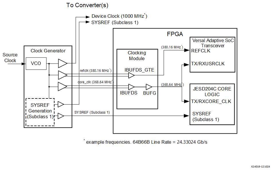
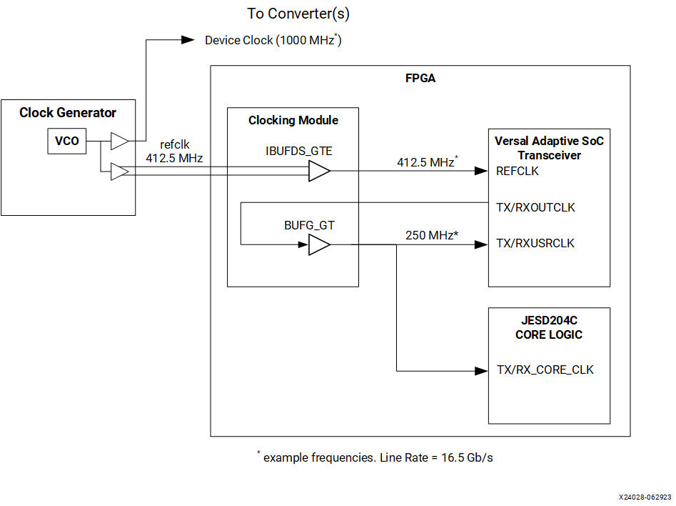
In 64b66b mode the JESD204C IP core requires both a 64-bit clock and a 66-bit clock for the gearbox of the encoder and decoder. The JESD204C core_clk supplies the 64-bit clock. The 66-bit clock (txusrclk/rxusrclk) is sourced from the Versal Adaptive SoC Transceiver outclock port via a buf_g_t. Generate the example design for an illustration of how to connect these clocks. In 8b10b mode no extra clocking is required.
AXI4-Lite Interface Clock
The JESD204C core is configured and monitored through an AXI4-Lite processor interface. The clock for this interface is separate and independent from the core and reference clocks. The AXI4-Lite clock must be a free running clock as it is also used to clock the reset circuitry. The valid range is between 10 MHz and 200 MHz.
DRP Clock for UltraScale+/UltraScale Devices
JESD204C system implementation requires the use of a JESD204 PHY core. The JESD204_PHY core must be supplied with a DRP clock (see JESD204 PHY LogicCORE IP Product Guide (PG198)).
Separate Transceiver Reference and Core Clocks
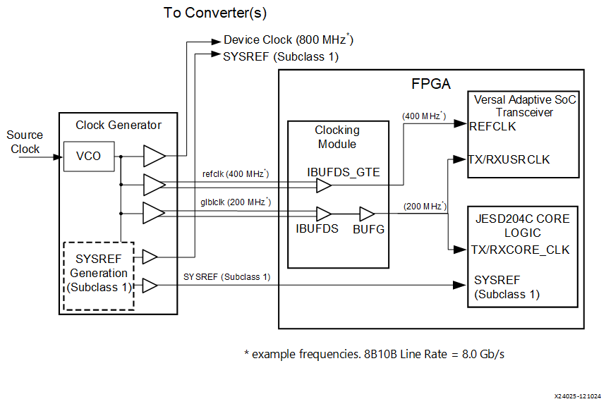
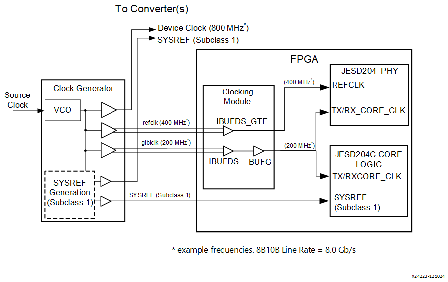
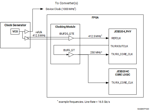
For JESD204C, the most generic and flexible clocking scheme uses separate transceiver reference and JESD204C core clocks supplied to the FPGA. In this configuration, the reference and core clocks are physically separate and can be run at independent, but related, frequencies, without additional constraints. The reference clock can be run at any frequency within the limitations of the transceiver for the selected line rate. The core clock always runs at the required rate (1/66th or 1/40th of the serial line rate). This configuration is shown in the following two figures for 64B66B and 8B10B line coding.
Transceiver Reference Clock Used as Core Clock
For some systems, it is possible to run a single clock input which acts as both the transceiver reference clock and the JESD204C core clock. While this configuration can sometimes simplify a system design, it is not always compatible.
For 64B66B systems in Versal adaptive SoCs, the required core clock frequency is usually not suitable for use as a reference clock for a Versal Adaptive SoC Transceiver configured to use the RPLL. Therefore, the LCPLL should be used if a single clock is required. In this configuration, the input transceiver reference clock must always be the required rate (1/66th of the serial line rate for 64B66B systems or 1/40th of the serial line rate for 8B10B systems).
For 64B66B systems in UltraScale+/UltraScale devices, the required core clock frequency is not suitable for use as a reference clock for a JESD204 PHY configured to use the CPLL (therefore QPLL 0 or 1 must be used if a single clock is required, or two clocks must be supplied if the CPLL must be used). In this configuration, the input transceiver reference clock must always be the required rate (1/66th of the serial line rate for 64B66B systems or 1/40th of the serial line rate for 8B10B systems).
Note: When using this clocking scheme in UltraScale+/UltraScale devices, the signal GT_POWERGOOD output from the JESD204_PHY must be connected to the CE pin on the BUFG_GT used to source core_clk from refclk.
The configurations are shown in the following figures.
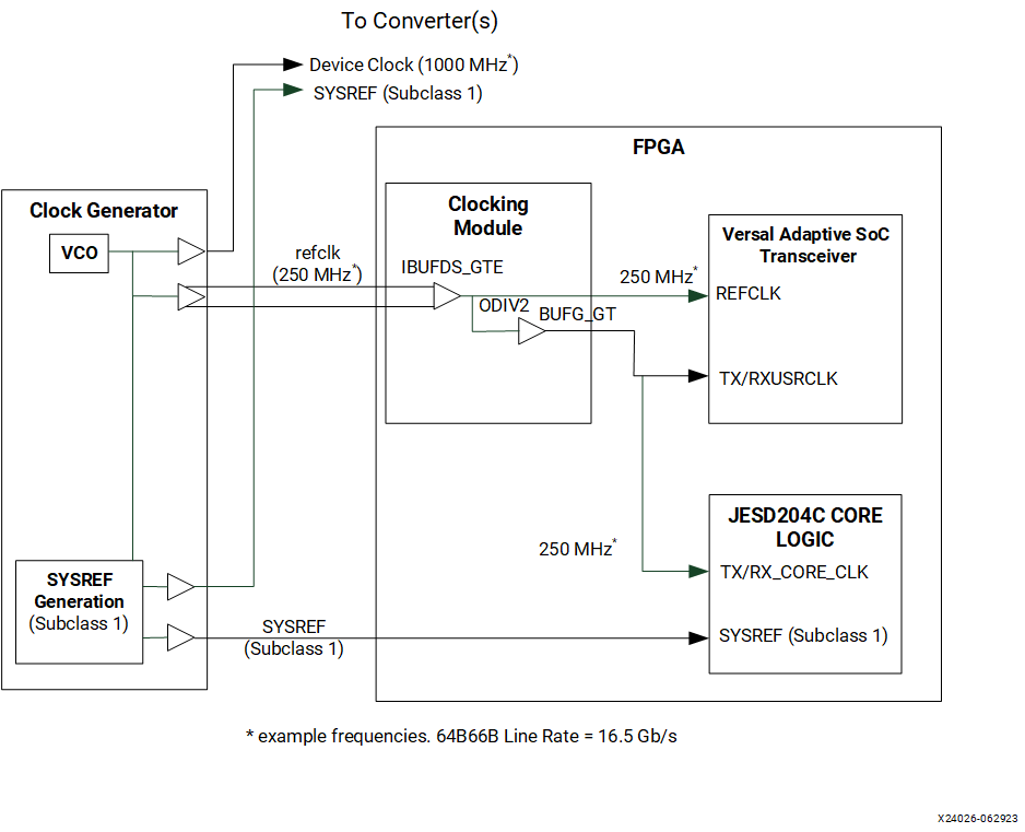
The ODIV2 output from the IBUFDS_GTE should be used to drive the I input of the BUFG_GT. Using the O output of the IBUFDS_GTE is not allowed and will result in a DRC error.
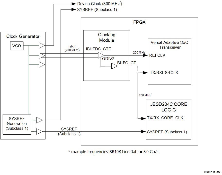
The ODIV2 output from the IBUFDS_GTE should be used to drive the I input of the BUFG_GT. Using the O output of IBUFDS_GTE is not allowed and will result in a DRC error.
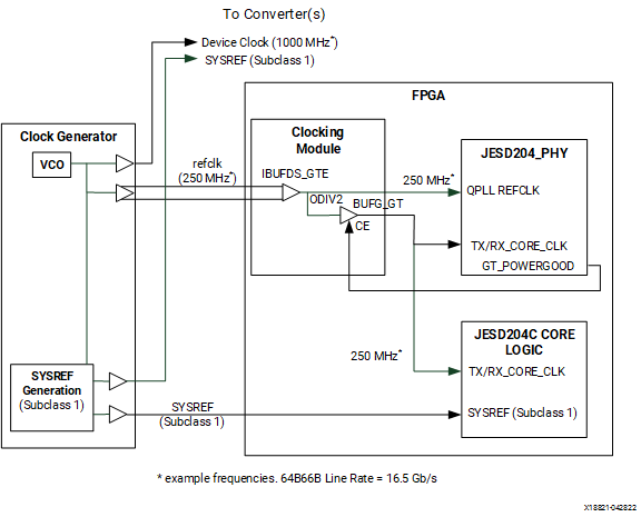
The ODIV2 output from the IBUFDS_GTE should be used to drive the I input of the BUFG_GT. Using the O output of IBUFDS_GTE is not allowed and will result in a DRC error.
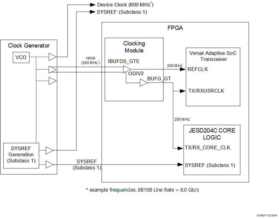
The ODIV2 output from the IBUFDS_GTE should be used to drive the I input of the BUFG_GT. Using the O output of IBUFDS_GTE is not allowed and will result in a DRC error.
Transceiver Output Clock Used as Core Clock
For Subclass 0 only operation, the timing limitations imposed to support deterministic latency are removed, and a simplified clocking arrangement can be used which requires only a reference clock input. In this case, the transceiver PLL is used to generate the core clock signal. In this configuration, any clock frequency that is suitable to use as the transceiver reference clock is acceptable. The Versal adaptive SoCs and UltraScale+/UltraScale device configurations are shown in the following figures.
This configuration is not suitable for subclass 1 or 2 operation because the output phase of the transceiver PLL is unknown, and therefore, this clock cannot be used to reliably sample SYSREF or SYNC.
Clocking Considerations
Always refer to the device data sheet for the chosen part and speed grade to confirm which PLLs are available for a required line rate; PLL selection for a particular rate might not be arbitrary.
Versal adaptive SoCs:
If the RPLL is required, the transceiver reference clock cannot be used as the core clock when the core is configured for 64B66B linecoding because the acceptable reference clock input frequencies to the RPLL do not cover the required Line Rate/66 ratio. This restriction does not apply when the core is configured for 8B10B linecoding.
UltraScale+/UltraScale:
If the CPLL is required, the transceiver reference clock cannot be used as the core clock when the core is configured for 64B66B linecoding because the acceptable reference clock input frequencies to the CPLL do not cover the required Line Rate/66 ratio. This restriction does not apply when the core is configured for 8B10B linecoding. For Line rates above 16.375 Gbps, ensure only port MGTREFCLK0 is used to drive QPLL0, and MGTREFCLK1 to drive QPLL1.