TI204c-IP User Guide
1 Overview
The JESD204C protocol (also known as JESD204 Revision C) is a high throughput data transfer protocol designed specifically for interfacing high speed data converters to logic devices like FPGAs and any ASICs that support the protocol. JESD is developed over the base infrastructure of the Ethernet Protocol, specifically the Physical, Data Link and Transport Layers. In addition, it incorporates additional features suited for data converters and acquisition/sampling related applications. These features allow for accurate synchronization and timing control over multiple physical lanes that the various JESD capable devices in the system may use to exchange data with each other.
The TI-204c FPGA IP has been developed by Texas Instruments for enabling fast and robust system development and bring-up of JESD links between TI data converters and FPGAs.
2 Terms and Definitions
| Term | Definition |
|---|---|
| Lane | A single channel of data between a transmitter and a receiver • Each lane physically represents a differential pair of signals that transmit serial data • Data for a converter channel may be transmitted on one or more lanes to trade off speed and number of differential pins/traces |
| Link | A combination of one or more lanes. • Lanes are synchronized within a link, but multiple links may not be synchronized across each other • One data converter device may contain one or more links |
| Line/Lane Rate | The data rate for a given link (usually expressed in Gigabits per second) |
| JESD204b | Revision B of the JESD204 protocol |
| ILAS | Initial Lane Alignment Sequence. • The transmitter sends the ILAS when bringing up the link in 8b/10b modes. Refer to the JESD204C specification for complete details. |
| JMODE / LMFS Mode | JESD Mode of the data converter • Each JESD capable TI data converter can support multiple data transfer modes, each with varying JESD link parameters. The parameters for a particular mode are referred to as a ‘JMODE’ or an ‘LMFS’ mode. • Please refer to the device datasheet for more information |
| SYSREF | This is the alignment signal used to synchronize the various Rx and Tx devices and links in a JESD system. |
Table 1. Terms and Definitions
3 TI204c IP Design Flow Methodology
The JESD protocol is fairly complex owing to the high data rates and multiple layers involved. As a result, it brings with it challenges in the areas of design, implementation and debug. This can often cause extended cycle times, either for system development and time to market, or for failure analysis of existing solutions. In some cases, engineers may choose an LVDS interface based solution, trading off perceived JESD bring-up effort vs board cost and complexity.
The TI 204c FPGA IP has been designed to minimize the overall time and effort required to implement a working link between a TI ADC and a host/application FPGA. This is accomplished by keeping most of the complexity of the protocol ‘under the hood’, requiring the user to provide a few configuration parameters that will optimize the IP for the JESD application being targeted. In addition, a generic reference design is provided as a starting point, which can then be modified to meet the actual application needs.
Design engineers using the TI204c IP are encouraged to follow the flow specified below. This will ensure a smooth and minimally time intensive transition from specifications to the final working JESD application. The steps are:
- Determine the JESD link parameters needed by your application
o Please refer to the JESD specifications of the chosen TI data converter for more information - Determine the FPGA of choice
o The FPGA selected should support the lane rates and transceiver counts required by the application - You will be provided a reference design that is customized for your application needs and targeted for a Xilinx development kit or a prototype FPGA boad. You can use it as a starting point to carry out the following (if necessary):
o Further customize the MGT transceiver block or re-map it for a different FPGA
o Further customize the JESD IP
o Edit the reference design to include logic specific to your application
o Edit/customize the synthesis and place-and-route constraints - Run the Vivado design flow to generate the bitfile for system bring-up and debug
3.1 JESD Link Parameters
The JESD link parameters should be determined based on the application needs and the JESD modes supported by the data converter.
- Sampling rate (Fs). This is the primary constraint of any data acquisition system. For a given link, a higher Fs will result in a higher data throughput requirement on the link
- Please refer to the JMODE/LMFS mode tables of the data converter datasheet to determine the Lane Rate corresponding to a given Fs.
- Number of lanes (L). Choosing a mode where a channel’s data is divided over multiple lanes will help reduce the overall line rate. The trade-off is higher routing resources on the board and more I/O resources on the FPGA
- Encoding protocol. The JESD standard offers two encoding protocols:
- The 8b/10b protocol guarantees DC balancing on the traces and also includes a number of error checking mechanisms for bit errors. However, it has two limitations
- There is a 20% bandwidth loss, as each 8bit code is converted to a 10bit representation. This results in a greater line rate requirement
- The transceivers are limited to approximately 16.375Gbps when carrying out 8b/10b decoding. This encoding is not recommended above 12.5Gbps, especially if DFE is enabled at the receiver.
- The 64b/66b protocol has a much smaller overhead and supports lane rates of up to 32Gbps. However, this is a relatively new inclusion in the JESD standard, so the number of data converters (and JESD modes within converters) supporting this mode may be less than the corresponding support for 8b/10b.
- The 8b/10b protocol guarantees DC balancing on the traces and also includes a number of error checking mechanisms for bit errors. However, it has two limitations
- Link synchronization and/or deterministic latency
- In certain applications, there may be a need to synchronize multiple links or multiple devices connected to one FPGA
- In other applications there may be one or more synchronized links, but there is an additional requirement that the end to end delay (front end of ADC to data output of the receive JESD IP in the FPGA) should remain defined and constant across all possible variations and across power cycles.
Once the JESD link modes have been determined, the designer should have the following parameters defined:
- L : number of lanes
- LR : Lane rate (Gbps)
- Encoding
- 8b/10b requires the following additional parameters
- F: Number of octets per frame
- K: Number of frames per multiframe
- 64b/66b requires the following
- E: Number of multi-blocks in an extended multi-block
- 8b/10b requires the following additional parameters
3.2 Determining the FPGA of choice
Once the JESD link parameters have been defined, choosing the FPGA will depend on a number of factors:
- The FPGA must support as many transceivers as the number of lanes required in the link(s)
- The FPGA transceivers must support the targeted line rate
- The transceivers must support the clock buffering and routing constraints imposed by the board level connections (which are usually optimized to keep costs low)
- The FPGA fabric must support adequate resources to accommodate both the JESD IP and the application logic (without over-burdening the routing, congestion and timing constraints that the tool needs to honor).
The UltraScale, UltraScale+ and 7000 series of families contain a variety of transceiver classes, named as GTY, GTH, GTX and GTP. The TI-204c IP is compatible with all of these classes, and generates the signals necessary to interface with and control the transceiver operation.
The TI204c-IP is compatible with the following Xilinx FPGAs.
- Xilinx Virtex™ UltraScale™ and UltraScale+™
- Xilinx Kintex™ UltraScale and UltraScale+
- Xilinx Zynq™ UltraScale+ and Zynq UltraScale+ (Auto)
- Xilinx Artix™ 7 and Artix 7 (Auto)
- Xilinx Virtex 7
- Xilinx Kintex 7 and Kintex 7 (Auto)
- Xilinx Zynq7000 and Zynq7000 (Auto)
Note: Pease refer to the official TI204c-IP page for the latest list of supported FPGAs, as it may get updated over time.
4 TI204c-IP High Level Block Diagram
4.1 Basic Block Diagram and Port List
Figure 1 below illustrates a simplified block diagram and minimal port list of the TI-204c JESD FPGA IP. While the entire IP is provided as encrypted SystemVerilog code, the transceiver instantiation module (marked in green) is left as regular source code. This is to enable the designer to make further customizations to the transceiver (if necessary).
The ports marked in red are the typical board level connections for the transceiver and consist of the following:
- Transceiver Reference Clock (one differential pair per clock buffer)
- Transceiver Data Rx/Tx Pins (one differential pair per lane)
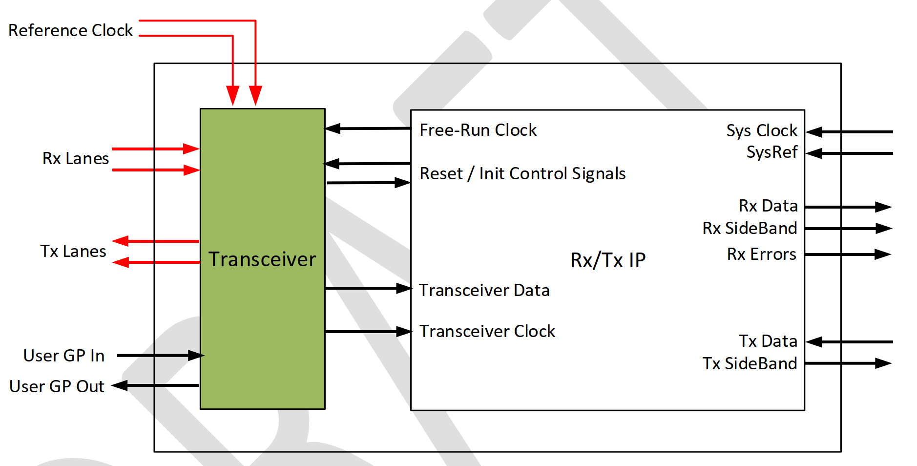
The ports on the right are connected to and controlled by the application logic in the FPGA. These fall into the following general categories:
- Clocks: These are the basic clocks needed to operate the IP
- Resets: These are the reset controls for initializing and IP and subsequently the JESD link
- Lane Specific signals: These form the actual data payload that is received over the JESD link
- Lane Rx/Tx Data: this is generated in 32/64/128 bit packets
- Sideband signals: These indicate frame / multiframe / multi-block and extended multi-block boundaries
- Error signals: These reflect lane specific error statistics and are 8b/10b or 64b/66b protocol dependent
- User GP In / Out : These are general purpose ports provided to the designer, and can be used for customized signaling between the transceiver and the rest of the application logic. The TI204c-IP does not use these signals for any of the internal functionality.
4.2 Integrated Rx Transport Layer
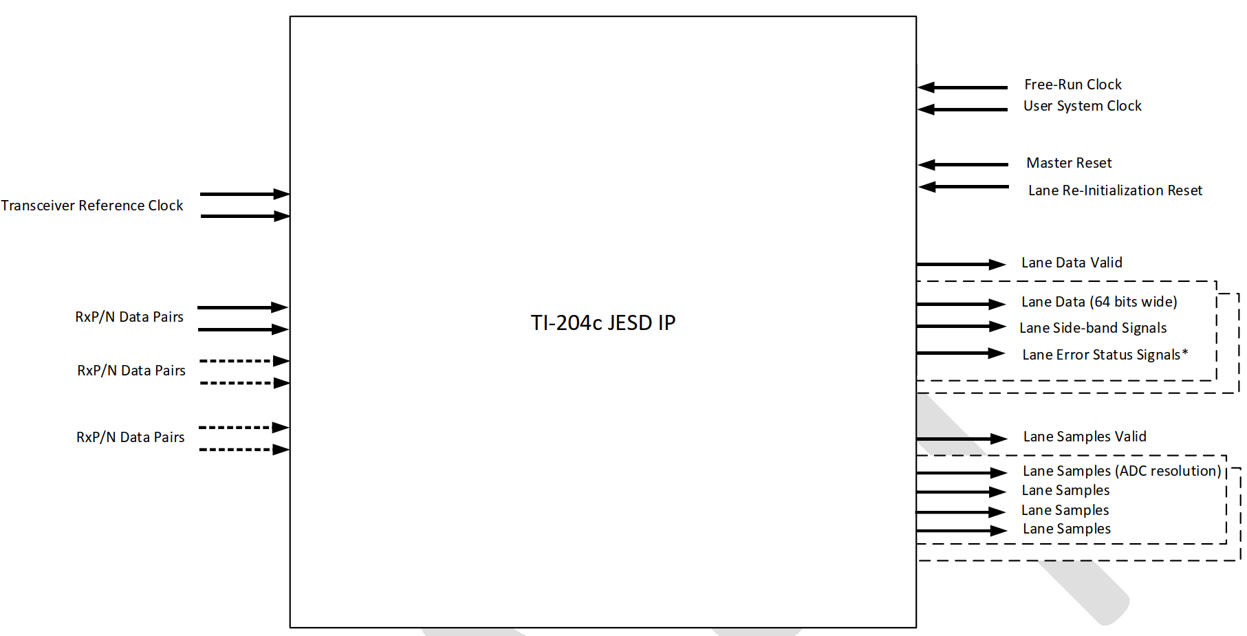
The JESD IP can also be generated with an integrated transport layer for the Rx IP that will interpret the lane data and output a desired number of samples per cycle on each lane. The FPGA designer can either use these samples for further processing, or choose to create a customized transport layer for generating the samples. The figure below illustrates an example where each lane emits 64 bit data per cycle, and the IP also has a corresponding output that exports 4 samples per cycle per lane (sorted and mapped as per the ADC resolution).
4.3 Block Diagram of the TI-204c IP
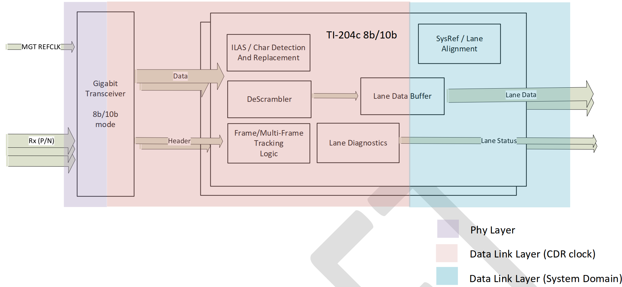
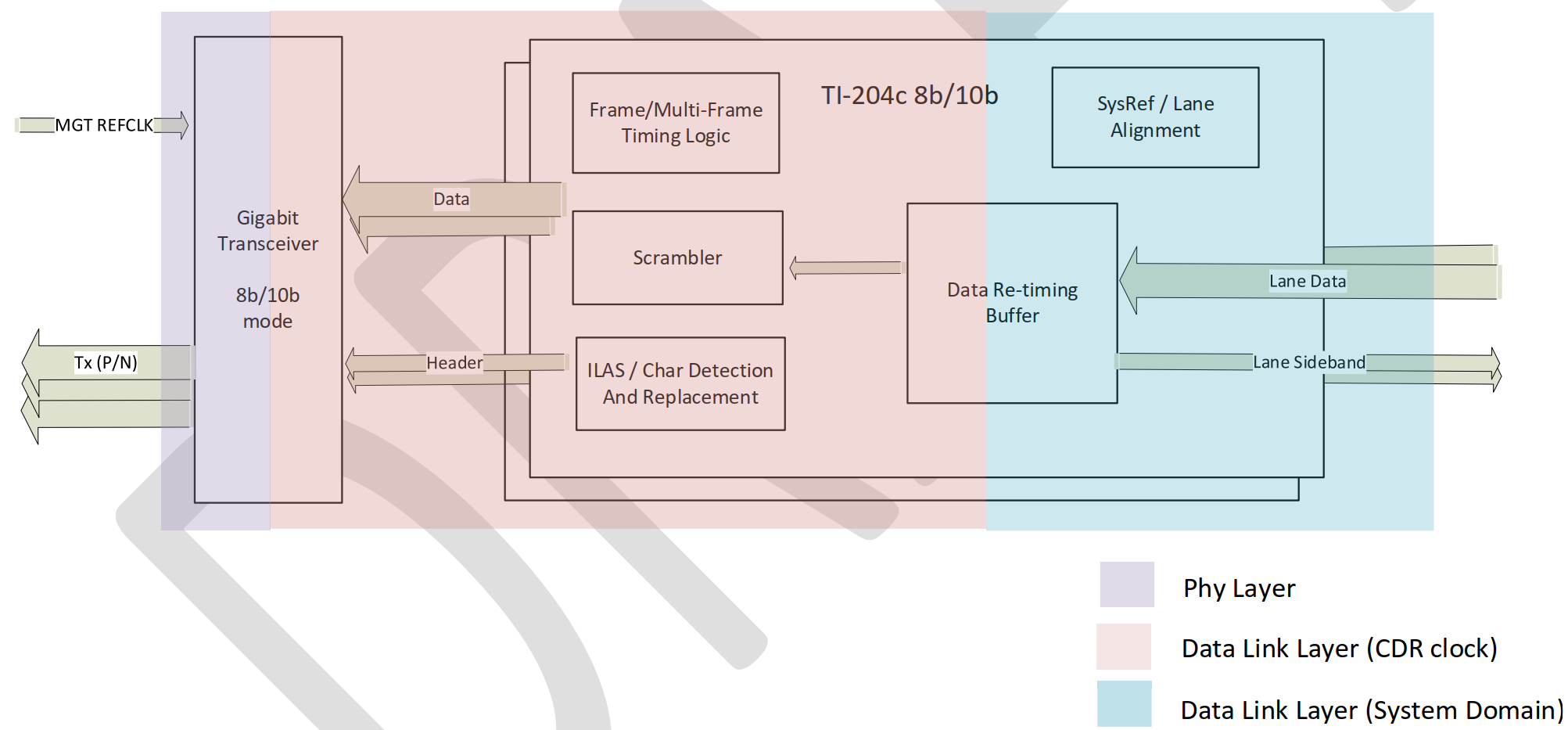
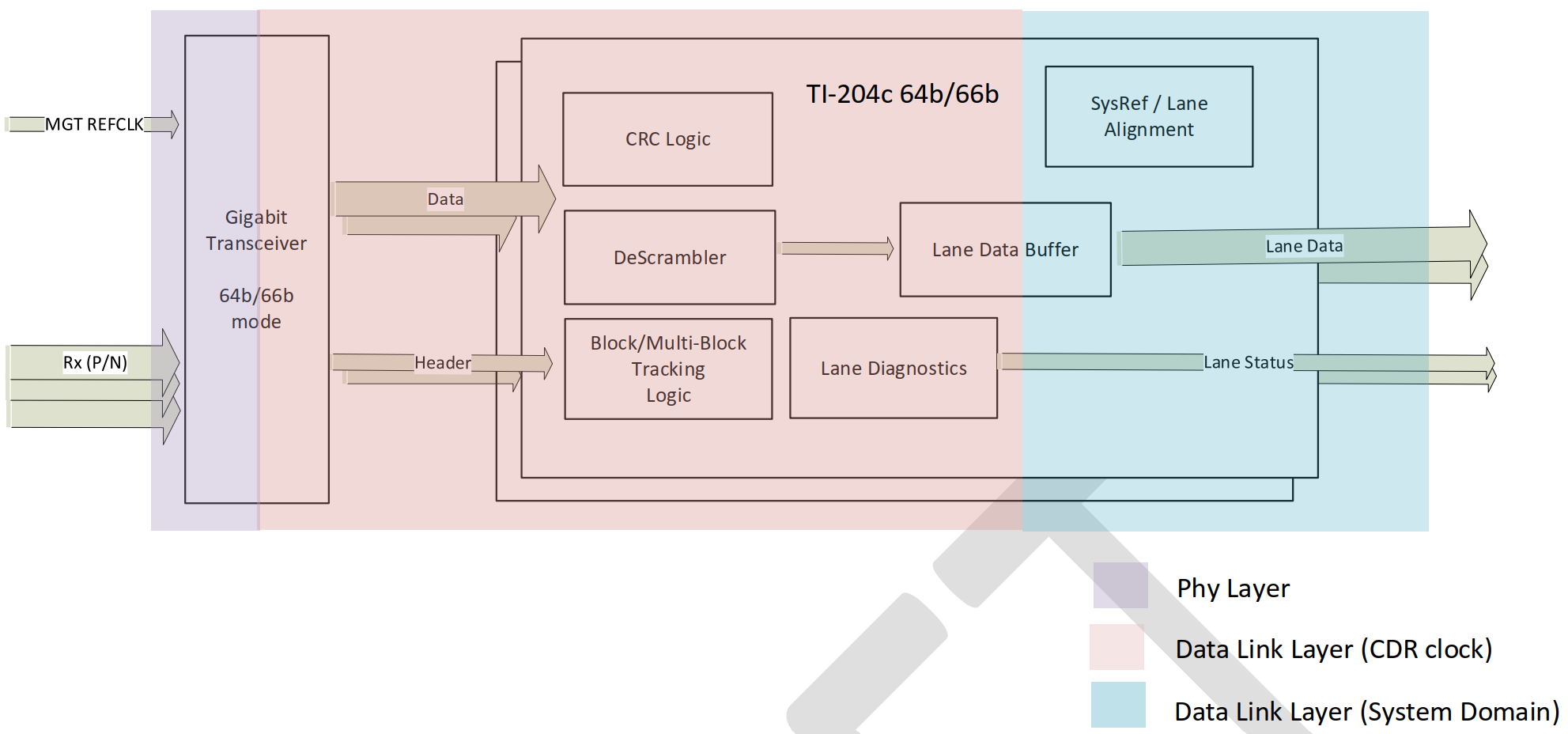
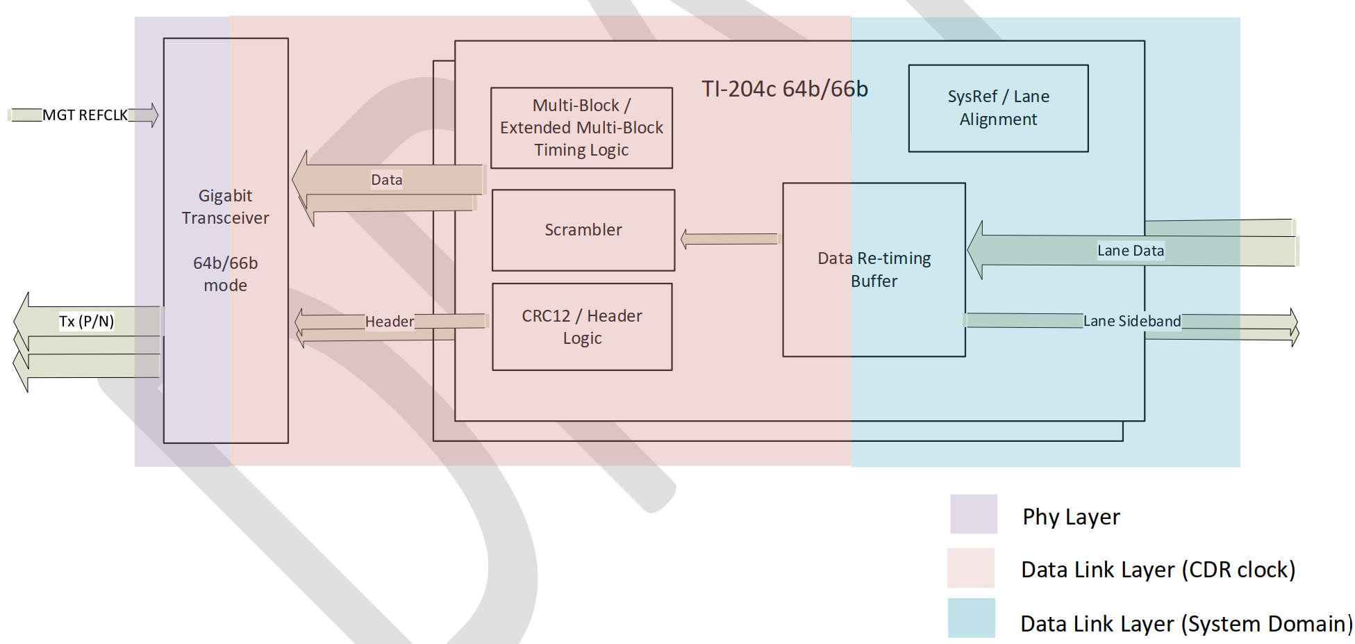
The following sub-sections illustrates the block diagram of the IP when configured in its various modes (Rx/Tx) with the two protocols (8b/10b and 64b/66b). The three colors indicate three independent clock domains:
- The domain in purple is the SERDES line rate domain and is restricted to being located within the transceiver.
- The domain in red/orange is where the primary protocol related data handling and error checking is carried out
- The domain in blue is the clock that interacts with the application logic.
The JESD IP has been architected to isolate the high speed domains of the protocol from the application logic, thereby relaxing inter-domain timing constraints and improving place and route runtimes for the tool.
4.3.1 Rx IP in 8b/10b mode
4.3.2 Tx IP in 8b/10b mode
4.3.3 Rx IP in 64b/66b mode
4.3.4 Tx IP in 64b/66b mode
5 TI204c-IP Attribute, Port and Register List
The TI-204c JESD IP is built using two primary components- The encrypted System Verilog (RTL) core of the IP. This is generic and includes all the functionality of the JESD data link layer. The core of the IP is non-specific and can be synthesized for any FPGA using the Vivado tool flow.
- The non-encrypted Transceiver Wrapper logic that instantiates the Transceiver IP. The Transceiver IP is extremely specific to the FPGA part chosen to the application and must be generated using the Vivado Transceiver Wizard. This wrapper is instantiated inside the IP core, and can be customized by the designer (if the transceiver is enhanced for functionality beyond that required by the core IP).
This section describes the Attribute, Port and Register lists of the top level TI204c-IP.
5.1 TI204c-IP Parameter / Attribute list
The following table lists all the parameters (attributes) of the JESD IP.
| Attribute Name | Default | Functionality / Description |
|---|---|---|
IP_ID | 0 | Integer value used to assign an ID to the IP. This ID is passed to the Verilog wrapper that contains the MGT transceiver instance. This can be used to select transceivers of different attributes, in case an FPGA design has multiple JESD IP's, with each IP containing a different transceiver |
IP_TYPE | "RXTX" | Controls the type of IP generated: • "RXTX": IP contains logic for both Rx and Tx JESD datapaths • "RX": IP contains logic for Rx JESD datapaths - Tx related attributes can be left at default - Tx related input ports can be tied to 0's - Tx related output ports are driven to defaults and can be left unconnected • "TX": IP contains logic for Tx JESD path - Rx related attributes can be left at default - Rx related input ports can be tied to 0's - Rx related output ports are driven to defaults and can be left unconnected |
IP_PROTOCOL | 810 | Controls the protocol supported by the IP • 810: IP contains logic for 8b/10b mode of the JESD protocol - 64b/66b related attributes can be left at default - 64b/66b related input ports can be tied to 0's - 64b/66b related output ports are driven to defaults • 6466: IP contains logic for 64b/66b mode of the JESD protocol - 8b/10b related attributes can be left at default - 8b/10b related input ports can be tied to 0's - 8b/10b related output ports are driven to defaults |
ADC_RES | 12 | Resolution of the ADC connected to the Rx IP |
DAC_RES | 12 | Resolution of the DAC connected to the Tx IP |
GT_TYPE | "GTYP" | Type of transceiver in the FPGA • GTYP : GTY transceiver, UltraScale+ device • GTY : GTY transceiver, UltraScale device • GTHP : GTH transceiver, UltraScale+ device • GTH : GTH transceiver, UltraScale device • GTX : GTX transceiver, 7000 series device • GTP : GTP transceiver, 7000 series device |
NUM_REFCLK_BUFFERS | 2 | Number of Reference Clock Buffer pins used for the MGT • This refers to the number of LVDS reference clock pairs only • The internal routing of reference clocks within/across the Quads of the transceiver may vary based on the application |
NUM_QUADS | 2 | Number of Quads used in the transceiver |
NUM_RX_LANES | 8 | Number of Rx channels / lanes used in the transceiver |
RX_LN_IDX_WIDTH | 3 | Log (base2) of NUM_RX_LANES (rounded up to nearest power of 2)• Eg: If NUM_RX_LANES = 4, RX_LN_IDX_WIDTH = 2• Eg: If NUM_RX_LANES = 12, RX_LN_IDX_WIDTH = 4 |
RX_LN_DATA_WIDTH | 64 | Data width of each lane of the Rx IP. Allowed values (and supported transceivers) are • 32 : GTYP, GTY, GTHP, GTH, GTX, GTP • 64 : GTYP, GTY, GTHP, GTH, GTX • 128 : GTYP (64b/66b mode only) |
NUM_TX_LANES | 8 | Number of Tx channels / lanes used in the transceiver |
TX_LN_IDX_WIDTH | 3 | Log (base2) of NUM_TX_LANES (rounded up to nearest power of 2)• E.g.: If NUM_TX_LANES = 4, TX_LN_IDX_WIDTH = 2• E.g.: If NUM_TX_LANES = 12, TX_LN_IDX_WIDTH = 4 |
TX_LN_DATA_WIDTH | 64 | Data width of each lane of the Tx IP. Allowed values (and supported transceivers) are • 32 : GTYP, GTY, GTHP, GTH, GTX, GTP • 64 : GTYP, GTY, GTHP, GTH, GTX • 128 : GTYP (64b/66b mode only) |
GT_USERIO_IN_WIDTH | 16 | Data width of the MGT transceiver related general purpose IN port |
GT_USERIO_OUT_WIDTH | 16 | Data width of the MGT transceiver related general purpose OUT port |
PARAM_RX_F | 1 | 'F' parameter of the 8b/10b protocol for the Rx IP. This indicates the number of octets per frame |
PARAM_RX_K | 32 | 'K' parameter of the 8b/10b protocol for the Rx IP. This indicates the number of frames per multi-frame. |
PARAM_RX_HD | 0 | 'HD' parameter of the 8b/10b protocol for the Rx IP. When set to '1', it indicates that the bits representing a sample are not contained entirely within one lane |
PARAM_TX_N | 16 | 'N' parameter of the 8b/10b protocol for the Tx IP |
PARAM_TX_NPR | 16 | 'Nprime' parameter of the 8b/10b protocol for the Tx IP |
PARAM_TX_CS | 0 | 'CS' parameter of the 8b/10b protocol for the Tx IP |
PARAM_TX_F | 1 | 'F' parameter of the 8b/10b protocol for the Tx IP |
PARAM_TX_K | 32 | 'K' parameter of the 8b/10b protocol for the Tx IP Note: The value of ( PARAM_TX_F * PARAM_RX_K * 8) must be an integral multiple of TX_LN_DATA_WIDTH. The K (or K minus 1) value in the DAC should be programmed in accordance with this requirement |
PARAM_TX_DEVID | 0 | 'DEVID' parameter of the 8b/10b protocol for the Tx IP |
PARAM_TX_BANKID | 0 | 'BANKID' parameter of the 8b/10b protocol for the Tx IP |
PARAM_TX_HD | 0 | 'HD' parameter of the 8b/10b protocol for the Tx IP |
PARAM_TX_M | 8 | 'M' parameter of the 8b/10b protocol for the Tx IP |
PARAM_TX_S | 4 | 'S' parameter of the 8b/10b protocol for the Tx IP |
PARAM_RX_E | 4 | 'E' parameter of the 64b/66b protocol for the Rx IP |
PARAM_TX_E | 1 | 'E' parameter of the 64b/66b protocol for the Tx IP |
RX_SYSREF_OFFSET | 0 | Number of sequential stages between the SYSREF at the input pin of the FPGA and the rx_sysref input pin of the JESD IP. This is applicable for designs requiring deterministic latency |
TX_SYSREF_OFFSET | 0 | Number of sequential stages between the SYSREF at the input pin of the FPGA and the tx_sysref input pin of the JESD IP. This is applicable for designs requiring deterministic latency |
RX_RBD_COUNT_WIDTH | 10 | Width of the delay counter used for controlling the buffer release timing of the Rx IP. This is applicable for designs requiring deterministic latency |
RX_LMFC_TARGET_COUNT | 0 | This value controls the number of rx_sys_clock cycles required for one period of the system multi-frame. This is reserved for 8b/10b encoding. This is applicable for designs requiring deterministic latencyIt is recommended that this value be set to 0, as the IP will compute the timing parameters internally. A non 0 value should be used only if either of the following conditions is true: - RX_LN_DATAWIDTH = 32, and rx_sys_clock is not LineRate/40- RX_LN_DATAWIDTH = 64, and rx_sys_clock is not LineRate/80 |
RX_LEMC_TARGET_COUNT | 0 | This value controls the number of rx_sys_clock cycles required for one period of the system extended multi-block. This is reserved for 64b/66b encoding. This is applicable for designs requiring deterministic latencyIt is recommended that this value be set to 0, as the IP will compute the timing parameters internally. A non 0 value should be used only if either of the following conditions is true: - RX_LN_DATAWIDTH = 32, and rx_sys_clock is not LineRate/33- RX_LN_DATAWIDTH = 64, and rx_sys_clock is not LineRate/66- RX_LN_DATAWIDTH = 128, and rx_sys_clock is not LineRate/132 |
RX_BUFFER_TYPE | "NORM" | This parameter should be left unmodified from the value in the reference design |
RX_BUFFER_RATIO | 1 | This parameter should be left unmodified from the value in the reference design |
TX_BUFFER_TYPE | "NORM" | This parameter should be left unmodified from the value in the reference design |
RX_TL_ENABLED | "NO" | This parameter should be left unmodified from the value in the reference design |
TL_PARAM1 | 1 | This parameter should be left unmodified from the value in the reference design |
TL_PARAM2 | 0 | This parameter should be left unmodified from the value in the reference design |
TL_PARAM3 | 1 | This parameter should be left unmodified from the value in the reference design |
SAMPLES_PER_CYCLE_PER_LANE | 4 | This parameter should be left unmodified from the value in the reference design |
TL_TYPE | "NORM" | This parameter should be left unmodified from the value in the reference design |
5.2 Port List
The following table lists the ports available on the IP. The tables have been divided to group signals of a common functionality together.
Top-Level Ports
| Signal Name | Width | Dir | Clock Domain | Functionality |
|---|---|---|---|---|
mgt_refclk_p | NUM_REFCLK_BUFFERS | IN | NA | Differential reference clock inputs to the MGT transceiver |
mgt_refclk_n | NUM_REFCLK_BUFFERS | IN | NA | Differential reference clock inputs to the MGT transceiver |
mgt_freerun_clock | 1 | IN | NA | Free-running clock input to the MGT transceiver. Used for initialization and reset control of the MGT. |
master_reset_n | 1 | IN | NA (Async) | Active-low asynchronous master reset for the entire IP, including the transceiver. |
mgt_lane_rxp | NUM_RX_LANES | IN | NA | Differential positive input for each Rx lane. |
mgt_lane_rxn | NUM_RX_LANES | IN | NA | Differential negative input for each Rx lane. |
mgt_lane_txp | NUM_TX_LANES | OUT | NA | Differential positive output for each Tx lane. |
mgt_lane_txn | NUM_TX_LANES | OUT | NA | Differential negative output for each Tx lane. |
gt_userio_in | GT_USERIO_IN_WIDTH | IN | NA | General purpose input bus connected directly to the transceiver wrapper. |
gt_userio_out | GT_USERIO_OUT_WIDTH | OUT | NA | General purpose output bus connected directly to the transceiver wrapper. |
rx_sys_clock | 1 | IN | NA | This is the system clock of the Rx IP. All output data and side-band signals are synchronous to this clock. Note: The frequency of this clock must be equal to or greater than the data generation rate of the Rx IP (to avoid data loss). The frequency of this clock is derived as follows: 8b10b modes: - If RX_LN_DATA_WIDTH = 32, Fsysclk >= LineRate/40- If RX_LN_DATA_WIDTH = 64, Fsysclk >= LineRate/8064b66b modes: - If RX_LN_DATA_WIDTH = 32, Fsysclk >= LineRate/33- If RX_LN_DATA_WIDTH = 64, Fsysclk >= LineRate/66- If RX_LN_DATA_WIDTH = 128, Fsysclk >= LineRate/132 |
rx_sync_reset | 1 | IN | rx_sys_clock | Synchronous reset for the Rx IP. When set to '1', it resets only the Data Link Layer of the Rx IP. Note: after power-up or a link loss event, it is recommended to hold rx_sync_reset at '1' after master_reset_n is deactivated from '1' to '0'. The rx_sync_reset should be held active until the PLL lock signals of the transceiver have transitioned to '1'. Note: the rx_sync_reset can be independently used for a quick clear and resync of all the lanes in the IP (without the additional latency of re-initializing the analog components in the transceiver). |
cfg_rx_lane_enable | NUM_RX_LANES | IN | NA (False Path) | Enable control for ADC lanes connected to the transceiver's Rx ports. The functionality of each bit is as follows: • 0 : Respective lane is enabled in the Rx IP • 1 : Respective lane is enabled in the Rx IP Note: This port should be tied to all '1's. However, it can be used to isolate and debug lane related issues if necessary. |
cfg_rx_lane_map | NUM_RX_LANES*3 bits (packed) | IN | NA (False Path) | Re-ordering control for ADC lanes connected to the transceiver's Rx ports. |
cfg_rx_lane_polarity | NUM_RX_LANES | IN | NA (False Path) | Polarity control for ADC lanes connected to the transceiver's Rx ports. |
mgt_rx_usrclk2 | 1 | OUT | NA | This is the usrclk2 clock generated by the transceiver. The frequency of this clock is derived as follows: 8b10b modes: - If RX_LN_DATA_WIDTH = 32, Fusrclk2 = LineRate/40- If RX_LN_DATA_WIDTH = 64, Fusrclk2 = LineRate/8064b66b modes: - If RX_LN_DATA_WIDTH = 32, Fusrclk2 = LineRate/33- If RX_LN_DATA_WIDTH = 64, Fusrclk2 = LineRate/66- If RX_LN_DATA_WIDTH = 128, Fusrclk2 = LineRate/132 |
Rx IP Status and Control Ports
| Signal Name | Width | Dir | Clock Domain | Functionality |
|---|---|---|---|---|
rx_all_lanes_locked | 1 | OUT | rx_sys_clock | When '1', indicates that all the lanes in the Rx IP have locked to the character / block boundaries embedded in their respective data streams from the transmitter. 8b/10b mode: Indicates that all lanes have aligned to the K char boundaries during the CGS phase. 64b/66b mode: Indicates that all lanes have aligned to the multi-block and extended multi-block boundaries in the data stream. Note: This signal can be used to detect and synchronize the release of Rx data lanes if there are multiple JESD Rx IP's in the FPGA. In the case of single IP designs, this signal can be left unused. |
rx_release_all_lanes | 1 | IN | rx_sys_clock | When set to '0', this holds the Rx IP from releasing the data lanes. When set to '1', this initiates the lane release sequence of the Rx IP on the subsequent LEMC / LMFC event, thus allowing the control of multiple Rx IP's to release in a synchronized manner. Note: In the case of multi JESD IP designs, this signal should transition from '0' to '1' after rx_all_lanes_locked output of all IP's has transitioned from '0' to '1'.Note: In case there is only one Rx IP in the design, this signal can be tied to '1'. Note: This signal does not guarantee deterministic latency. It only guarantees a synchronized release of all lanes across multiple JESD Rx IPs in the FPGA. |
rx_lane_data | Array: NUM_RX_LANES of width RX_LN_DATA_WIDTH | OUT | rx_sys_clock | Output data buses of the Rx IP. There is one output bus per transceiver lane. Note: All the lanes within one JESD Rx will release in a synchronized manner. |
rx_lane_valid | 1 | OUT | rx_sys_clock | Data valid signal for the output lane data and sideband signals of the Rx IP. • When '1', it indicates that the new data and sideband signals are valid and can be used by the downstream logic for processing. • When '0', the last valid values of the data and sideband signals will be held. These values should be discarded from downstream processing. The rx_lane_valid signal will intermittently transition from '1' to '0' if the frequency of rx_sys_clock (Fsysclk) is greater than the minimum value described in this table. If the Fsysclk is maintained at the minimum value, the data valid will always remain '1' after the lanes have released. |
rx_lane_buffer_overflow | NUM_RX_LANES | OUT | mgt_rx_usrclk2 | When set to '1', this indicates that the data buffer of the respective lane has encountered an overflow, thereby resulting in a loss of data. Note: This is a sticky flag and will be cleared only by a sync reset or master reset, as it requires a re-sync of all the lanes of the Rx IP before samples can reliably be extracted from the rx_lane_data outputs of the Rx IP. |
rx_lane_samples | 3D array: NUM_RX_LANES arrays, each containing SAMPLES_PER_CYCLE_PER_LANE values of ADC_RES | OUT | rx_sys_clock | Output of the internal transport layer of the JESD Rx IP. This consists of the lane data, sorted into separate samples and packed into the required number of samples per cycle. Note: This is an advanced feature of the JESD Rx IP and will be provided with the customized reference design. Note: The embedded transport layer may not be available for all JESD modes of the various data converters from TI. Note: The embedded transport layer may add a latency between the lane data and the final output samples. If this latency is not desirable, the designer is encourage to create customized logic to map the lane data to samples. |
rx_lane_samples_valid | NUM_RX_LANES | OUT | rx_sys_clock | When ‘1’, indicates that the values on the rx_lane_samples bus are valid. Note: All the bits of the rx_lane_samples_valid output will transition to ‘0’ to ‘1’ simultaneously. If this is not the case, it indicates that samples from one (or more)of the lanes may be out of sync with the rest. |
rx_sync_n | 1 | OUT | rx_sys_clock | SYNCn output of the JESD Rx IP. This is valid only in 8b/10b mode. |
cfg_rx_scrambling_enabled | 1 | IN | NA (false path) | When ‘1’ enables the de-scrambling feature of the Rx IP. |
rx_lane_configuration_data | Array: NUM_RX_LANES of 112 bits each | OUT | mgt_rx_usrclk2 | These are the 14 concatenated ILAS configuration octets received on each lane of the Rx IP. The octets are arranged in increasing order in the 112 bit bus, with octet 0 at bits 7:0 and octet 13 at bits 111:104. Note: The value of this output is updated just once after the ILAS phase, and retained until the next reset/re-sync event. |
rx_lane_start_of_frame | Array: NUM_RX_LANES of RX_LN_DATA_WIDTH/8 bits each | OUT | rx_sys_clock | This output accompanies the rx_lane_data and qualifies the corresponding byte as a start of frame delimiter. This value is valid only when rx_lane_data_valid is ‘1’. |
rx_lane_start_of_multiframe | Array: NUM_RX_LANES of RX_LN_DATA_WIDTH/8 bits each | OUT | rx_sys_clock | This output accompanies the rx_lane_data and qualifies the corresponding byte as a start of multi-frame delimiter. This value is valid only when rx_lane_data_valid is ‘1’. |
rx_lane_start_of_mblock | NUM_RX_LANES | OUT | rx_sys_clock | This output accompanies the rx_lane_data and qualifies the most significant byte of the current rx_lane_data bus as a start of multi-block delimiter. This value is valid only when rx_lane_data_valid is ‘1’. |
rx_lane_start_of_emblock | NUM_RX_LANES | OUT | rx_sys_clock | This output accompanies the rx_lane_data and qualifies the most significant byte of the current rx_lane_data bus as a start of extended multi-block delimiter. This value is valid only when rx_lane_data_valid is ‘1’. |
rx_lane_crc_error | NUM_RX_LANES | OUT | rx_sys_clock | This output accompanies the rx_lane_data and indicates a CRC comparison error on the last received CRC value in the header stream and the computed CRC of the previous multi-block. |
rx_clr_all_err_count | 1 | IN | mgt_rx_usrclk2 | When set to ‘1’, this will clear all the independent 8b/10b and 64b/66b error counts exported by the IP. |
Rx IP Error Counters
| Signal Name | Width | Dir | Clock Domain | Functionality |
|---|---|---|---|---|
rx_lane_invalid_somf_err_count | Array: NUM_RX_LANES of 4 bits each | OUT | mgt_rx_usrclk2 | Number of invalid ‘start of multi-frame’ events detected in the receive stream for the respective lane. Note: This will stop incrementing at the max value of 'hF. |
rx_lane_clr_invalid_somf_err_count | NUM_RX_LANES | IN | mgt_rx_usrclk2 | When set to ‘1’, clears the rx_lane_invalid_somf_err_count value for the respective lane. |
rx_lane_invalid_eomf_err_count | Array: NUM_RX_LANES of 4 bits each | OUT | mgt_rx_usrclk2 | Number of invalid ‘end of multi-frame’ events detected in the receive stream for the respective lane. Note: This will stop incrementing at the max value of 'hF. |
rx_lane_clr_invalid_eomf_err_count | NUM_RX_LANES | IN | mgt_rx_usrclk2 | When set to ‘1’, clears the rx_lane_invalid_eomf_err_count value for the respective lane. |
rx_lane_invalid_eof_err_count | Array: NUM_RX_LANES of 4 bits each | OUT | mgt_rx_usrclk2 | Number of invalid ‘end of frame’ events detected in the receive stream for the respective lane. Note: This will stop incrementing at the max value of 'hF. |
rx_lane_clr_invalid_eof_err_count | NUM_RX_LANES | IN | mgt_rx_usrclk2 | When set to ‘1’, clears the rx_lane_invalid_eof_err_count value for the respective lane. |
rx_lane_notintable_err_count | Array: NUM_RX_LANES of 4 bits each | OUT | mgt_rx_usrclk2 | Number of ‘not in table’ events detected in the receive stream for the respective lane. Note: This will stop incrementing at the max value of 'hF. |
rx_lane_clr_notintable_err_count | NUM_RX_LANES | IN | mgt_rx_usrclk2 | When set to ‘1’, clears the rx_lane_notintable_err_count value for the respective lane. |
rx_lane_disp_err_count | Array: NUM_RX_LANES of 4 bits each | OUT | mgt_rx_usrclk2 | Number of ‘8b/10b running disparity error’ events detected in the receive stream for the respective lane. Note: This will stop incrementing at the max value of 'hF. |
rx_lane_clr_disp_err_count | NUM_RX_LANES | IN | mgt_rx_usrclk2 | When set to ‘1’, clears the rx_lane_disp_err_count value for the respective lane. |
rx_lane_invalid_header_err_count | Array: NUM_RX_LANES of 4 bits each | OUT | mgt_rx_usrclk2 | Number of ‘invalid header error’ events detected in the receive stream for the respective lane. Note: This will stop incrementing at the max value of 'hF. |
rx_lane_clr_invalid_header_err_count | NUM_RX_LANES | IN | mgt_rx_usrclk2 | When set to ‘1’, clears the rx_lane_invalid_header_err_count value for the respective lane. |
rx_lane_eomb_err_count | Array: NUM_RX_LANES of 4 bits each | OUT | mgt_rx_usrclk2 | Number of out of position end of multi-block events detected in the receive stream for the respective lane. Note: This will stop incrementing at the max value of 'hF. |
rx_lane_clr_eomb_err_count | NUM_RX_LANES | IN | mgt_rx_usrclk2 | When set to ‘1’, clears the rx_lane_eomb_err_count value for the respective lane. |
rx_lane_eoemb_err_count | Array: NUM_RX_LANES of 4 bits each | OUT | mgt_rx_usrclk2 | Number of out of position end of extended multi-block events detected in the receive stream for the respective lane. Note: This will stop incrementing at the max value of 'hF. |
rx_lane_clr_eoemb_err_count | NUM_RX_LANES | IN | mgt_rx_usrclk2 | When set to ‘1’, clears the rx_lane_eoemb_err_count value for the respective lane. |
rx_lane_crc_mismatch_err_count | Array: NUM_RX_LANES of 4 bits each | OUT | mgt_rx_usrclk2 | Number of CRC mismatch events detected in the receive stream for the respective lane. Note: This will stop incrementing at the max value of 'hF. |
rx_lane_clr_crc_mismatch_err_count | NUM_RX_LANES | IN | mgt_rx_usrclk2 | When set to ‘1’, clears the rx_lane_crc_mismatch_err_count value for the respective lane. |
Rx IP SYSREF and Alignment Ports
| Signal Name | Width | Dir | Clock Domain | Functionality |
|---|---|---|---|---|
rx_sysref | 1 | IN | rx_sys_clock | A positive edge detect on this signal is treated as a SYSREF event in the JESD Rx IP. |
rx_lmfc_pulse | 1 | OUT | rx_sys_clock | Single cycle pulse, indicating an LMFC (multi-frame boundary) event in the JESD Rx IP. Note: This is applicable only in 8b/10b mode. |
rx_lemc_pulse | 1 | OUT | rx_sys_clock | Single cycle pulse, indicating an LEMC (extended multi-block boundary) event in the JESD Rx IP. Note: This is applicable only in 64b/66b mode. |
rx_sysref_realign_count | 4 | OUT | rx_sys_clock | Indicates the number of times a SYSREF event caused a re-alignment of the LMFC/LEMC timing in the JESD Rx IP (after the last reset event). This stops incrementing after a reaching a max value of 'hF. |
rx_clr_sysref_realign_count | 1 | IN | rx_sys_clock | When ‘1’, clears the rx_sysref_realign_count. |
Rx IP Deterministic Latency Ports
| Signal Name | Width | Dir | Clock Domain | Functionality |
|---|---|---|---|---|
cfg_rx_det_latency_en | 1 | IN | NA (False Path) | Enable control for deterministic latency. The functionality of the bit is as follows: • 0: Rx IP lanes release together as soon as data is available in the buffer of each lane. • 1: Rx IP lanes release after data is available AND the cfg_rx_buffer_release_delay value is reached. |
cfg_rx_buffer_release_delay | RX_RBD_COUNT_WIDTH | IN | rx_sys_clock (false path) | This value determines the exact LMFC/LEMC cycle on which the Rx IP will release its lanes. The delay value is measured from the LMFC/LEMC pulse where the rx_release_all_lanes transition from '0' to '1' is observed.Note: This is applicable only if cfg_rx_det_latency_en = 1. |
rx_lmfc_to_buffer_release_delay | RX_RBD_COUNT_WIDTH | OUT | rx_sys_clock | This output is a profiling counter that indicates the number of cycles required by the Rx IP to release its data after the rx_release_all_lanes input is asserted.Note: This output value is valid only when cfg_rx_det_latency_en = 0. |
rx_lemc_to_buffer_release_delay | RX_RBD_COUNT_WIDTH | OUT | rx_sys_clock | This output is a profiling counter that indicates the number of cycles required by the Rx IP to release its data after the rx_release_all_lanes input is asserted.Note: This output value is valid only when cfg_rx_det_latency_en = 0. |
Tx IP Clocks and Resets
| Signal Name | Width | Dir | Clock Domain | Functionality |
|---|---|---|---|---|
cfg_tx_lane_map | NUM_TX_LANES*3 bits (packed) | IN | NA (False Path) | Re-ordering control for DAC lanes connected to the transceiver's Tx ports. |
cfg_tx_lane_polarity | NUM_TX_LANES | IN | NA (False Path) | Polarity control for DAC lanes connected to the transceiver's Tx ports. |
mgt_tx_usrclk2 | 1 | OUT | NA | This is the usrclk2 clock generated by the transceiver. The frequency of this clock is derived as follows:8b10b modes: - If TX_LN_DATA_WIDTH = 32, Fusrclk2 = LineRate/40- If TX_LN_DATA_WIDTH = 64, Fusrclk2 = LineRate/8064b66b modes: - If TX_LN_DATA_WIDTH = 32, Fusrclk2 = LineRate/33- If TX_LN_DATA_WIDTH = 64, Fusrclk2 = LineRate/66- If TX_LN_DATA_WIDTH = 128, Fusrclk2 = LineRate/132 |
tx_sys_clock | 1 | IN | NA | This is the system clock of the Tx IP. All input data and output side-band signals are synchronous to this clock. Note: The frequency of this clock must be equal to the data consumption rate of the Tx IP (to avoid data loss). The frequency of this clock is derived as follows: 8b10b modes: - If TX_LN_DATA_WIDTH = 32, Fsysclk = LineRate/40- If TX_LN_DATA_WIDTH = 64, Fsysclk = LineRate/8064b66b modes: - If TX_LN_DATA_WIDTH = 32, Fsysclk = LineRate/33- If TX_LN_DATA_WIDTH = 64, Fsysclk = LineRate/66- If TX_LN_DATA_WIDTH = 128, Fsysclk = LineRate/132 |
tx_sync_reset | 1 | IN | tx_sys_clock | Synchronous reset for the Tx IP. When set to '1', it resets only the Data Link Layer of the Tx IP. Note: after power-up or a link loss event, it is recommended to hold tx_sync_reset at '1' after master_reset_n is deactivated from '1' to '0'. The rx_sync_reset should be held active until the PLL lock signals of the transceiver have transitioned to '1'.Note: the tx_sync_reset can be independently used for a quick clear and resync of all the lanes in the IP (without the additional latency of re-initializing the analog components in the transceiver). |
cfg_tx_lane_enable | NUM_TX_LANES | IN | NA (False Path) | Enable control for DAC lanes connected to the transceiver's Tx ports. The functionality of each bit is as follows: • 0: Respective lane is enabled in the Tx IP • 1: Respective lane is enabled in the Tx IP Note: This port should be tied to all '1's. However, it can be used to isolate and debug lane related issues if necessary. |
Tx IP Data Ports
| Signal Name | Width | Dir | Clock Domain | Functionality |
|---|---|---|---|---|
tx_lane_data | Array: NUM_TX_LANES of width TX_LN_DATA_WIDTH | IN | tx_sys_clock | Input data buses of the Tx IP. There is one input bus per transceiver lane. Note: All the lanes within one JESD Tx will consume data in a synchronized manner. |
tx_lane_data_ready | 1 | OUT | tx_sys_clock | Data ready signal for the input lane data and output sideband signals of the Tx IP. • When '1', it indicates that the sideband signals are valid and that the upstream logic should drive the relevant data on the tx_lane_data inputs. |
tx_sync_n | 1 | IN | tx_sys_clock (false path) | SYNCn input of the JESD Tx IP. Note: This signal is internally synchronized and sampled by the IP logic. |
cfg_tx_scrambling_enabled | 1 | IN | NA (false path) | When '1' enables the data scrambling feature of the Tx IP. Note: This must be tied to '1'. The current version of the TI204c IP does not support 8b/10b Tx mode with scrambling disabled. |
cfg_tx_ilas_test_mode | 1 | IN | NA (false path) | When '1' configures the JESD Tx IP to continuously transmit the ILA sequence. |
Tx IP Sideband Signals
| Signal Name | Width | Dir | Clock Domain | Functionality |
|---|---|---|---|---|
tx_lane_start_of_frame | TX_LN_DATA_WIDTH/8 | OUT | tx_sys_clock | This output accompanies and qualifies the corresponding byte of the tx_lane_data as a start of frame delimiter. |
tx_lane_start_of_multiframe | TX_LN_DATA_WIDTH/8 | OUT | tx_sys_clock | This output accompanies and qualifies the corresponding byte of the tx_lane_data as a start of multi-frame delimiter. |
tx_lane_start_of_mblock | NUM_TX_LANES | OUT | tx_sys_clock | This output accompanies and qualifies the most significant byte of each lane of the current tx_lane_data bus as a start of multi-block delimiter. |
tx_lane_start_of_emblock | NUM_TX_LANES | OUT | tx_sys_clock | This output accompanies and qualifies the most significant byte of each lane of the current tx_lane_data bus as a start of extended multi-block delimiter. |
Tx IP SYSREF and Alignment Ports
| Signal Name | Width | Dir | Clock Domain | Functionality |
|---|---|---|---|---|
tx_sysref | 1 | IN | tx_sys_clock | A positive edge detect on this signal is treated as a SYSREF event in the JESD Tx IP. |
tx_lmfc_pulse | 1 | OUT | tx_sys_clock | Single cycle pulse, indicating an LMFC (multi-frame boundary) event in the JESD Tx IP. Note: This is applicable only in 8b/10b mode. |
tx_lemc_pulse | 1 | OUT | tx_sys_clock | Single cycle pulse, indicating an LEMC (extended multi-block boundary) event in the JESD Tx IP. Note: This is applicable only in 64b/66b mode. |
tx_sysref_realign_count | 4 | OUT | tx_sys_clock | Indicates the number of times a SYSREF event caused a re-alignment of the LMFC/LEMC timing in the JESD Tx IP (after the last reset event). This stops incrementing after reaching a max value of 'hF. |
tx_clr_sysref_realign_count | 1 | IN | tx_sys_clock | When ‘1’, clears the tx_sysref_realign_count. |
Reserved Test Ports
| Signal Name | Width | Dir | Clock Domain | Functionality |
|---|---|---|---|---|
testport1_in | 256 | IN | NA | Reserved. Must be tied to all 0’s. |
testport1_out | 256 | OUT | NA | Reserved. Leave unconnected. |
testport2_in | 256 | IN | NA | Reserved. Must be tied to all 0’s. |
testport2_out | 256 | OUT | NA | Reserved. Leave unconnected. |
testport3_in | 1050 | IN | NA | Reserved. Must be tied to all 0’s. |
testport3_out | 1050 | OUT | NA | Reserved. Leave unconnected. |
5.3 Register list
The TI204c-IP does not contain any registers, and hence does not implement a programming read/write interface. All the status and error signals are available as ports, ensuring minimal latency between the detection of an event and its update at the output of the IP. This latency is typically higher if the status is updated into a register that needs to be accessed by the application.
Any port that is tied to a static value or not connected to the application upstream/downstream will automatically result in the associated IP logic getting optimized during synthesis. This guarantees that the IP has the minimal required impact on the FPGA logic and routing resources.
6 TI204c-IP Design Notes
This section describes and illustrates the various design specific care-abouts of the TI204c JESD IP. Each sub-section is dedicated to a unique feature or aspect of the IP, and is intended to guide the designer through the steps and options for further customizing and optimizing the IP for the targeted application.
6.1 Transceiver Instantiation and Customization Guidelines
The following block diagram illustrates the instantiation of the Transceiver in the TI204c JESD IP core. The transceiver is embedded within the design and instantiated in a wrapper module with one of the following names:
- In the case of 8b/10b designs, the wrapper module is called "mgt_8b/10b_wrap". It instantiates the 8b/10b Transceiver IP.
- In the case of 64b/66b designs, the wrapper module is called "mgt_64b66b_wrap". It instantiates the 64b/66b Transceiver IP.
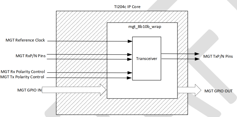
This is the only module in the JESD IP core that is not encrypted, and allows the designer the ability to customize the Transceiver IP for purposes that may be very specific to the application.
6.1.1 Transceiver Wrapper Module design guidelines
The transceiver wrapper module couples tightly with the control and data paths of the TI204c JESD IP core, and care should be taken to ensure that its instantiation within the IP core does not get affected by the customizations that are carried out. The following guidelines are essential for retaining proper functionality:
- The name of the wrapper (
mgt_xxxx_wrap) must be left unchanged. - The parameters of the module are directly inferred from the top level parameters of the JESD IP core, and must be left unchanged.
- The MGT GPIO in and out signals can be used by the designer for control/access to signals of the transceiver and for custom logic that is added to the transceiver wrapper. An example of this is adding DRP (configuration) ports to the transceiver IP, which can then be controlled/accessed from outside the JESD IP core through the GPIO ports.
The reference designs included in this user guide offer various Transceiver instantiation examples, and can be used as a starting point for further design development and customization.
6.2 Transceiver Reference Clock Setup and Data Pin Mapping Rules
The transceiver IP is generated using the Transceiver wizard tool in Vivado. This is a packaged IP that is instantiated inside the TI204c JESD IP, and hence it is important to ensure the correct mapping of reference clock and data pins of the FPGA to the appropriate pins of the ADC / DAC / clock buffers in the system. This section explains the various mapping nomenclature rules used by the Transceiver wizard for the final Transceiver IP that is generated.
6.2.1 Reference Design mapping example.
The following figure illustrates an 8 lane GTY transceiver example where the selected lanes are chosen from QuadX0Y0 and Quad X0Y1:
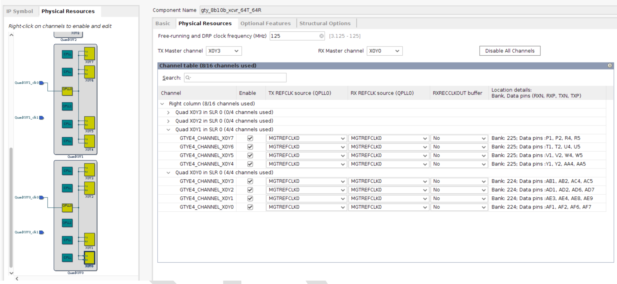
In the case above, the Vivado Transceiver Wizard will generate the transceiver IP (named gty_8b10b_xcvr_64T64R). The generated transceiver IP will order/name the lanes based on the channel numbering, and the same order will apply to the JESD IP ports:
- The 8 Rx and Tx lanes are part of the 8 channels in Quads X0Y0 and X0Y1
- The channel GTYE4_X0Y0 will be referenced as Lane 0
- The
mgt_lane_rxp/n[0]input port of the JESD IP will in turn be Lane 0 of the JESD Rx IP. This will map to FPGA pins AF2 and AF1 respectively - The
mgt_lane_txp/n[0]output port of the JESD IP will in turn be Lane 0 of the JESD Tx IP. This will map to FPGA pins AF7 and AF6 respectively
- The
- The channel GTYE4_X0Y1 will be referenced as Lane 1
- The
mgt_lane_rxp/n[1]input port of the JESD IP will in turn be Lane 1 of the JESD Rx IP. This will map to FPGA pins AE4 and AE3 respectively - The
mgt_lane_txp/n[1]output port of the JESD IP will in turn be Lane 1 of the JESD Tx IP. This will map to FPGA pins AE9 and AE8 respectively
- The
- And so on... until
- The channel GTYE4_X0Y7 will be referenced as Lane 7
- The
mgt_lane_rxp/n[7]input port of the JESD IP will in turn be Lane 7 of the JESD Rx IP. This will map to FPGA pins P2 and P1 respectively - The
mgt_lane_txp/n[7]output port of the JESD IP will in turn be Lane 7 of the JESD Tx IP. This will map to FPGA pins R5 and R4 respectively
- The
Each Quad's QPLL0 will receive its input from the respective Quad's MGTREFCLK0 input pin.
Important: Note that the name used for the transceiver IP is just an example. It can be modified, as long as the same instance name is used in the mgt_xxxx_wrap module.
6.2.2 Modified mapping example
The following figure illustrates an 8T/8R transceiver. This time, the 8 lanes chosen are split across 3 Quads (and not contiguous).
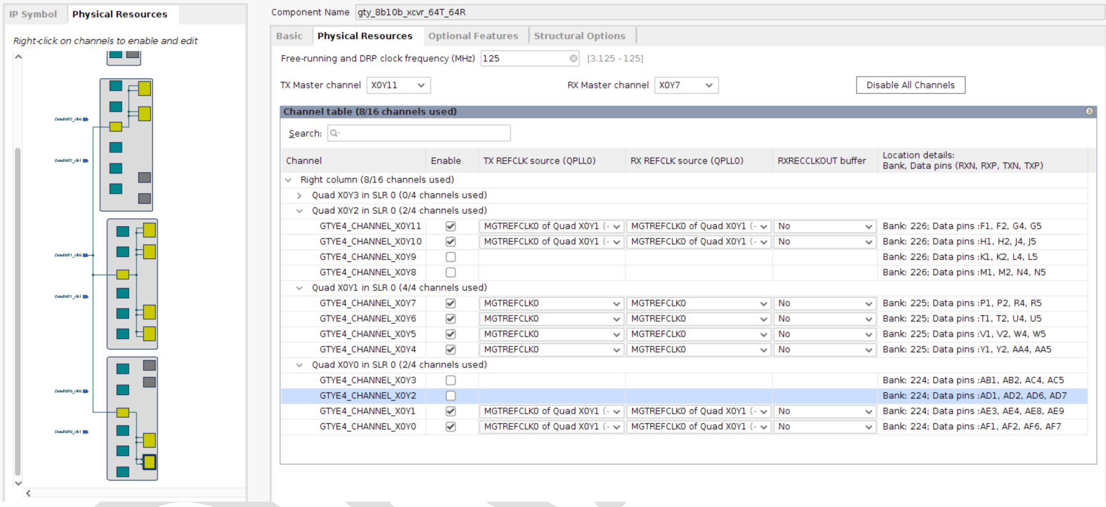
In the modified case, the generated transceiver IP will order/name the lanes based on the channel order from low to high. It is extremely important to note this, in order to ensure the correct mapping of the transceiver IP lanes to the top level ports of the TI204c JESD IP.
-
The 8 Rx and Tx lanes are selected from Quads X0Y0, X0Y1 and X0Y2
-
The channel GTYE4_X0Y0 will be referenced as Lane 0
- The
mgt_lane_rxp/n[0]input port of the JESD IP will in turn be Lane 0 of the JESD Rx IP. This will map to FPGA pins AF2 and AF1 respectively - The
mgt_lane_txp/n[0]output port of the JESD IP will in turn be Lane 0 of the JESD Tx IP. This will map to FPGA pins AF7 and AF6 respectively
- The
-
The channel GTYE4_X0Y1 will be referenced as Lane 1
- The
mgt_lane_rxp/n[1]input port of the JESD IP will in turn be Lane 1 of the JESD Rx IP. This will map to FPGA pins AE4 and AE3 respectively - The
mgt_lane_txp/n[1]output port of the JESD IP will in turn be Lane 1 of the JESD Tx IP. This will map to FPGA pins AE9 and AE8 respectively
- The
-
The channel GTYE4_X0Y4 will be referenced as Lane 2
- The
mgt_lane_rxp/n[2]input port of the JESD IP will in turn be Lane 2 of the JESD Rx IP. This will map to FPGA pins Y2 and Y1 respectively - The
mgt_lane_txp/n[2]output port of the JESD IP will in turn be Lane 2 of the JESD Tx IP. This will map to FPGA pins AA5 and AA4 respectively
- The
-
And so on... until
-
The channel GTYE4_X0Y11 will be referenced as Lane 7
- The
mgt_lane_rxp/n[7]input port of the JESD IP will in turn be Lane 7 of the JESD Rx IP. This will map to FPGA pins F2 and F1 respectively - The
mgt_lane_txp/n[7]output port of the JESD IP will in turn be Lane 7 of the JESD Tx IP. This will map to FPGA pins G5 and G4 respectively
- The
-
There is only one MGTREFCLK0 pin used in the FPGA, and that is the REFCLK0 pin of QuadX0Y1
- This clock buffer is connected to the QPLL0 of QuadX0Y1 and also feeds north and south to feed the QPLL0's of QuadX0Y2 and QuadX0Y0 respectively
- The transceiver IP generated by the transceiver Wizard will still define a 3 port reference clock input, but the GTYE4_IBUFDS clock buffer is expected to be connected to all three ports in the transceiver wrapper file.
6.3 Pin Mapping guidelines between the ADC/DAC and the JESD IP (FPGA)
The TI204c JESD IP offers integrated features to address both mapping and polarity related irregularities. All the data lanes of an ADC/DAC may not be connected to the respective counterpart lanes of the Rx/Tx lanes of the FPGA (JESD IP) in the correct order or polarity. Due to board design and routing challenges, it is often possible that one (or both) of the following occur on some of the lanes:
- The lanes aren't a direct 1-1 map between the FPGA and the data converter. For example, Lane 0 of the ADC is not routed to Rx Lane 0 of the JESD IP (on the FPGA). Instead, Lane 0 of the ADC is connected to Lane 4 of the Rx IP. Similarly, Lane 2 of a DAC may be routed to Lane 5 of the Tx IP on the FPGA. a. Such mapping irregularities can make the final FPGA design challenging, because it can be difficult to accurately map the data transmitted / received on lanes to the respective converter sample values.
- There may be polarity inversions between the transmitter and the receiver. For example, the TxP output pin of a certain lane of the transmitter (i.e. the FPGA's Tx IP) is connected to the RxN input pin of the receiver lane of the DAC. a. Polarity inversions will typically cause lane initialization to fail in 64b/66b modes. However, in 8b/10b mode, the encoding protocol may mask the inversion by allowing the link to get established, but the sample values will be corrupted.
6.3.1 Pin mapping for ADC connected to an Rx IP
The following image illustrates an 8 lane ADC connected to an 8 lane Rx IP in the FPGA. The symbol  illustrates a polarity inversion.
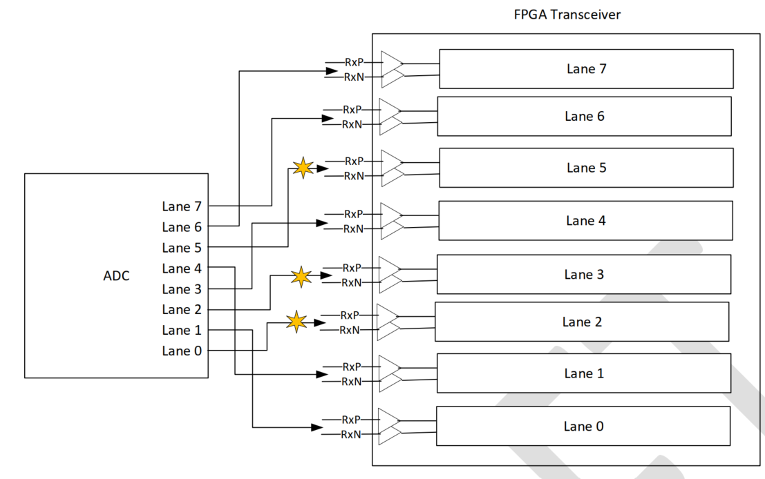
The mapping is represented in the following table:
| ADC Lane Number | FPGA Rx IP Lane Number | Inversion (Y/N) |
|---|---|---|
| 0 | 2 | Y |
| 1 | 0 | N |
| 2 | 3 | Y |
| 3 | 4 | N |
| 4 | 1 | N |
| 5 | 5 | Y |
| 6 | 7 | N |
| 7 | 6 | N |
The above mapping will result in the following port values for the JESD IP:
cfg_rx_lane_map = {3'd6, 3'd7, 3'd5, 3'd1, 3'd4, 3'd3, 3'd0, 3'd2}
cfg_rx_lane_polarity = 8'b00100101
Note: The values should be based on the perspective of the lanes of the ADC (ordered from highest to lowest).
6.3.2 Pin mapping for DAC connected to a Tx IP
The following image illustrates an 8 lane DAC connected to an 8 lane Tx IP in the FPGA. The symbol illustrates a polarity inversion.
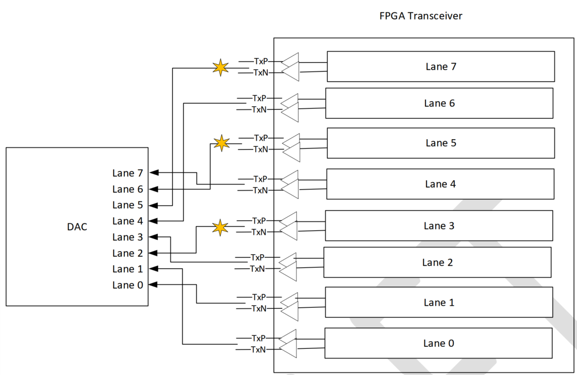
The mapping is represented in the following table:
| DAC Lane Number | FPGA Tx IP Lane Number | Inversion (Y/N) |
|---|---|---|
| 0 | 1 | N |
| 1 | 0 | N |
| 2 | 3 | Y |
| 3 | 2 | N |
| 4 | 6 | N |
| 5 | 7 | Y |
| 6 | 5 | Y |
| 7 | 4 | N |
The above mapping will result in the following port values for the JESD IP:
cfg_tx_lane_map = {3'd4, 3'd5, 3'd7, 3'd6, 3'd2, 3'd3, 3'd0, 3'd1}
cfg_tx_lane_polarity = 8'b01100100
Note: The values should be based on the perspective of the lanes of the DAC (ordered from highest to lowest).
6.4 IP Clock guidelines
The JESD IP contains the following clock related inputs and outputs:
6.4.1 MGT Free-running Clock
The transceiver IP requires a free-running clock for basic initialization and reset control. This is usually a low frequency clock and does not have strict jitter requirements, and can hence be provided from any clock source available in the FPGA. However, it is important that the clock is stable before the master reset of the JESD IP is released.
The frequency of this clock can be chosen in the transceiver wizard. An example is the 125MHz setting illustrated in Mapping of Selected Transceiver Channels. The allowed range of the clock is also listed in the same parameter window of the Transceiver Wizard.
6.4.2 MGT Reference Clock (input)
This is the set of inputs that drive the reference clock to the MGT transceiver clocking resources (QPLLs / CPLLs). These must be connected to the MGTREFCLK pins of the FPGA. The following figure illustrates the typical topology of clocks within a Quad (4 channel group). Note that this figure applies to the GTH and GTY class transceivers. The GTX and GTP class may have a different architecture.
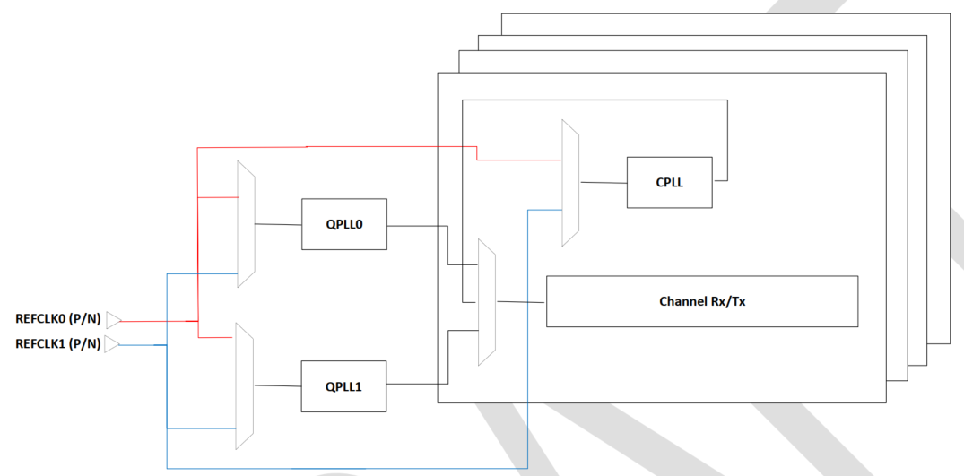
As illustrated in Figure 1: Typical Clocking Topology for a Quad the final clock used for data extraction can be selected from the QPLL0 or QPLL1 or the CPLL. Each PLL has a range of operation, and the designer must refer to the guidelines in the respective datasheet of the FPGA and the transceiver User Guide.
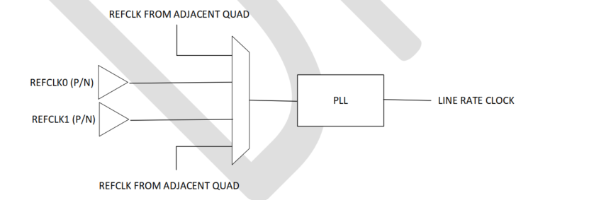
Furthermore, the PLLs may receive their reference clock either directly from the REFCLK pins of the same Quad or from adjacent Quads. This is illustrated in Figure 2: Reference clock options for the QPLL0/QPLL1/CPLL.
6.4.3 MGT generated Rx IP clock (output) :
This is the clock generated by the Rx channels in the transceiver, and can be used to drive logic in the FPGA fabric. This is internally driven by a BUFG and does not require any additional clock buffer instantiations outside the JESD IP.
6.4.4 MGT generated Tx IP clock (output):
This is the clock (mgt_tx_usrclk2) generated by the Tx channels in the transceiver, and can be used to drive logic in the FPGA fabric. The frequency of this clock is derived from the Line Rate and is described in the table below:
| Encoding protocol | TX_LN_DATA_WIDTH | Frequency |
|---|---|---|
| 8b/10b | 32 | LineRate/40 |
| 8b/10b | 64 | LineRate/80 |
| 64b/66b | 32 | LineRate/33 |
| 64b/66b | 64 | LineRate/66 |
| 64b/66b | 128 | LineRate/132 |
Note: The mgt_tx_usrclk2 is internally driven by a BUFG and does not require any additional clock buffer instantiation outside the JESD IP.
6.4.5 MGT generated Rx IP clock (output):
This is the clock (mgt_rx_usrclk2) generated by the Rx channels in the transceiver, and can be used to drive logic in the FPGA fabric. The frequency of this clock is derived from the Line Rate and is described in the table below:
| Encoding protocol | RX_LN_DATA_WIDTH | Frequency |
|---|---|---|
| 8b/10b | 32 | LineRate/40 |
| 8b/10b | 64 | LineRate/80 |
| 64b/66b | 32 | LineRate/33 |
| 64b/66b | 64 | LineRate/66 |
| 64b/66b | 128 | LineRate/132 |
Note: The mgt_rx_usrclk2 is internally driven by a BUFG and does not require any additional clock buffer instantiation outside the JESD IP.
6.4.6 Tx IP System Clock (tx_sys_clock)
The tx_sys_clock drives the blue domain illustrated in the Tx IP block diagrams in the TI204c-IP High Level Block Diagram section of this user guide. This is the primary domain used for interaction between the JESD Tx IP and the upstream application logic.
The tx_sys_clock frequency is fixed based on the IP configuration and is described below:
| Encoding protocol | TX_LN_DATA_WIDTH | Frequency |
|---|---|---|
| 8b/10b | 32 | LineRate/40 |
| 8b/10b | 64 | LineRate/80 |
| 64b/66b | 32 | LineRate/33 |
| 64b/66b | 64 | LineRate/66 |
| 64b/66b | 128 | LineRate/132 |
Notes:
- The
tx_sys_clockcan be driven by themgt_tx_usrclk2output of the JESD IP, as the frequencies are exactly identical. However, this is encouraged only for designs that do not need deterministic latency, which involves accurate sampling of the SYSREF input pin for synchronizing timing between the transceiver and receiver. - If deterministic latency is required, the
tx_sys_clockshould be sourced independently through a dedicated clock capable input pin of the FPGA, which will allow tight control of its timing with respect to the SYSREF pin. If thetx_sys_clockis sourced independently, it should still be generated from a common root clock being used to generate DAC as well as the MGTREFx clocks. This will ensure that any drift in the clock impacts all the components together.
6.4.7 Rx IP System Clock (rx_sys_clock)
The rx_sys_clock drives the blue domain illustrated in the various figures in the Rx IP block diagrams of the TI204c-IP High Level Block Diagram section of this user guide. This is the primary domain used for interaction between the JESD Rx IP and the downstream application logic.
The rx_sys_clock frequency has a lower limit based on the IP configuration and is described below:
| Encoding protocol | RX_LN_DATA_WIDTH | Frequency (should be equal to or greater than the following) |
|---|---|---|
| 8b/10b | 32 | LineRate/40 |
| 8b/10b | 64 | LineRate/80 |
| 64b/66b | 32 | LineRate/33 |
| 64b/66b | 64 | LineRate/66 |
| 64b/66b | 128 | LineRate/132 |
Notes:
- The
rx_sys_clockcan be driven by themgt_rx_usrclk2output of the JESD IP, as the frequencies are exactly identical. However, this is encouraged only for designs that do not need deterministic latency, which involves accurate sampling of the SYSREF input pin for synchronizing timing between the transceiver and receiver. - If deterministic latency is required, the
rx_sys_clockshould be sourced independently through a dedicated clock capable input pin of the FPGA, which will allow tight control of its timing with respect to the SYSREF pin. If therx_sys_clockis sourced independently, there are two options:- If the frequency is exactly at the lower limit as per the table above, it should still be generated from a common root clock being used to generate ADC as well as the MGTREFx clocks. This will ensure that any drift in the clock impacts all the components together.
- If the frequency is greater than the lower limit as per the table above, it can be generated using any clock source available in the FPGA. In this case, the IP will de-activate the
rx_data_validsignal and hold the data on all the lanes whenever one or more lanes have an empty buffer.
6.5 Mapping of Rx/Tx lane data to ADC/DAC samples
The TI204c JESD IP has been architected to enable an easy and straightforward mapping of the data-converter samples to the respective data ports of the Rx and Tx IPs. This is carried out by implementing a 1-1 correlation between the JMODE/LMFS table of the data-converter and the rx_lane_data and tx_lane_data ports of the JESD IP. This, in turn, enables an easy sorting of ADC samples for downstream data processing or easy mapping of upstream samples to the Tx IP for transmission to the DAC.
6.5.1 Mapping of Rx Lane Data to ADC samples
The following figure illustrates the JMODE0 and JMODE30 output format of the ADC12DJ5200RF ADC. JMODE0 is an 8b/10b protocol, while JMODE30 is a 64b/66b protocol. In both cases the ADC generates 12 bit samples that are packed into the 8 lanes as shown in the table below. The important points to note are:
- The table defines a 64 bit frame (per lane)
- Each lane has 4 tail bits after every 60 bits (5 samples per 64 bit packet)
- 8 lanes create a total of 40 samples in each frame
- The samples are arranged from S0 to S39, with S0 appearing on Lane 0, S1 on Lane 4, S2 on Lane 2 and so on
Table 27. JMODE 0 (12-bit, Single Channel, DDC Bypass, 8 lanes)
| LANE | OCTET 0-1 (NIB 0-3) | OCTET 2-3 (NIB 4-7) | OCTET 4-5 (NIB 8-11) | OCTET 6-7 (NIB 12-15) | OCTET 8-9 (NIB 16-19) | OCTET 10-11 (NIB 20-23) | OCTET 12-13 (NIB 24-27) | OCTET 14-15 (NIB 28-31) |
|---|---|---|---|---|---|---|---|---|
| DA0 | S[0] | S[8] | S[16] | S[24] | S[32] | T | T | T |
| DA1 | S[2] | S[10] | S[18] | S[26] | S[34] | T | T | T |
| DA2 | S[4] | S[12] | S[20] | S[28] | S[36] | T | T | T |
| DA3 | S[6] | S[14] | S[22] | S[30] | S[38] | T | T | T |
| DB0 | S[1] | S[9] | S[17] | S[25] | S[33] | T | T | T |
| DB1 | S[3] | S[11] | S[19] | S[27] | S[35] | T | T | T |
| DB2 | S[5] | S[13] | S[21] | S[29] | S[37] | T | T | T |
| DB3 | S[7] | S[15] | S[23] | S[31] | S[39] | T | T | T |
Table 27 also applies to JMODE 30.
The waveforms below illustrate the data output by the Rx IP when connected to the ADC (configured to JMODE0). For the purpose of clarity, the waveform shows a total of 120 samples, A0 through A39, B0 through B39 and C0 through C39.
6.5.1.1 Data mapping with 64 bit Rx IP
The following waveform is the rx_lane_data output of the Rx IP (with RX_LN_DATA_WIDTH set to 64).
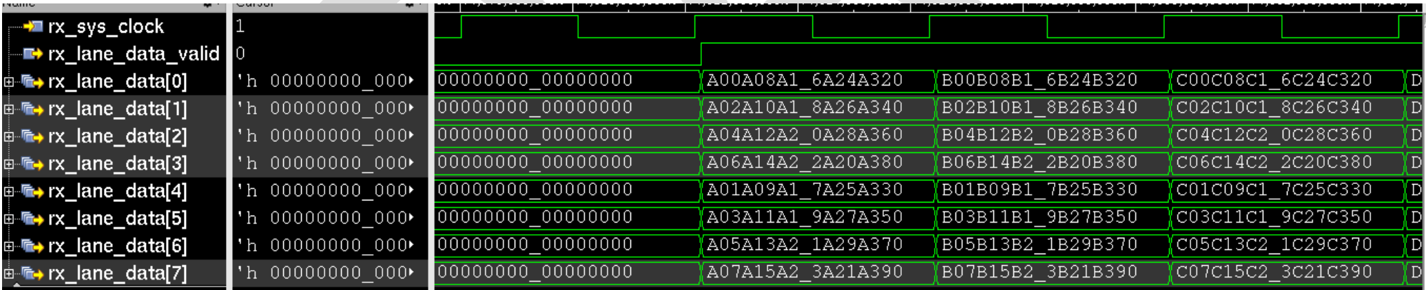
The transition of rx_lane_data_valid indicates the start of data from the Rx IP, showing that all the lanes release in an aligned manner.
The reader should be able to see a direct 1-1 correlation between the sample ordering on the rx_lane_data buses and the JMODE table. On each lane, each 64 bit packet has 4 tail bits of 'h0 at the LSB nibble.
6.5.1.2 Data mapping with 32 bit Rx IP
The following waveform is the rx_lane_data output of the Rx IP (with RX_LN_DATA_WIDTH set to 32).
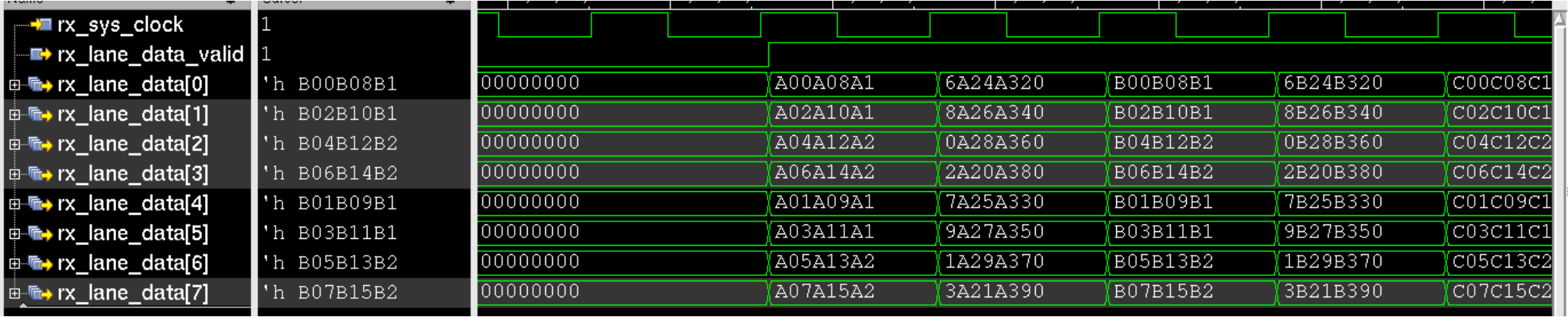
The transition of rx_lane_data_valid indicates the start of data from the Rx IP, showing that all the lanes release in an aligned manner. The reader should still be able to see a direct 1-1 correlation between the sample ordering on the rx_lane_data buses and the JMODE table. On each Lane, the 64 bit packet is now received in two consecutive cycles of 32 bit each. The 4 tail bits still occur after every 60 bits.
6.5.1.3 Data mapping with 128 bit Rx IP
The following waveform is the rx_lane_data output of the Rx IP (with RX_LN_DATA_WIDTH set to 128).
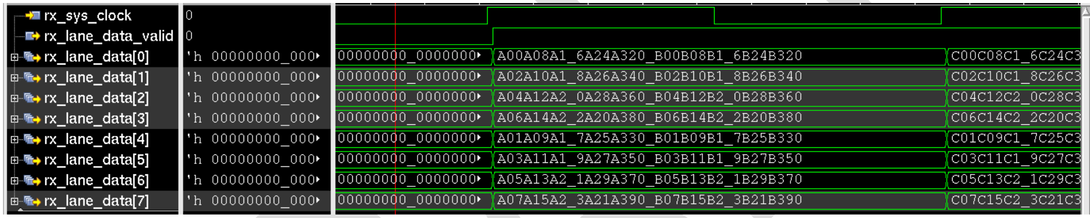
The transition of rx_lane_data_valid indicates the start of data from the Rx IP, showing that all the lanes release in an aligned manner. The reader should still be able to see a direct 1-1 correlation between the sample ordering on the rx_lane_data buses and the JMODE table. On each Lane, two 64 bit packets are received in each rx_sys_clock cycle. The 4 tail bits still occur after every 60 bits.
6.5.2 Mapping of DAC samples to Tx Lane Data
The following figure illustrates the LMFS = 8411 input format of the DAC38J84 data converter. The DAC is a two channel device with 16 bit samples that are packed into the 8 lanes as shown in the table. The important points to note are:
- Each sample is split across 2 lanes.
- Lanes 0-3 map the I channel, while Lanes 4-7 map the Q channel
Table 10. JESD204B Frame Assembly Byte Representation (Dual-Channel)
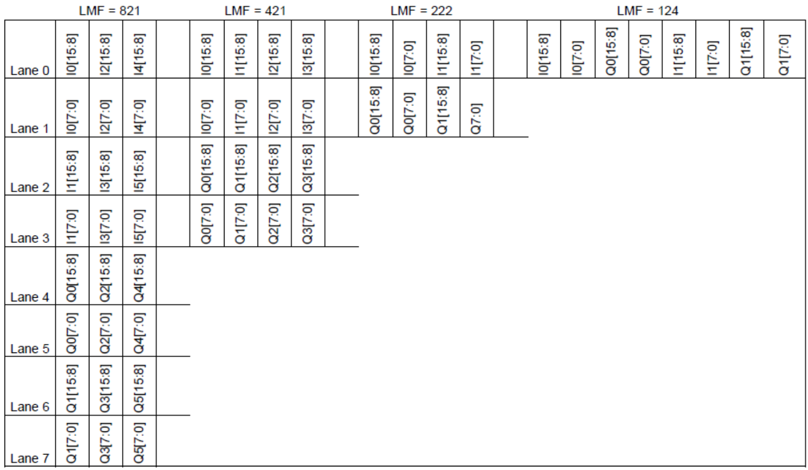
The waveforms below illustrate the data input to the Tx IP when connected to the DAC (configured to LMFS = 8411). For the purpose of clarity, the waveform shows a total of 48 samples on each channel. The I channel samples are AB00 through AB47, while the Q channel samples are CD00 through CD47.
6.5.2.1 Data mapping with 64 bit Tx IP
The following waveform is the tx_lane_data input to the Tx IP (with TX_LN_DATA_WIDTH set to 64).
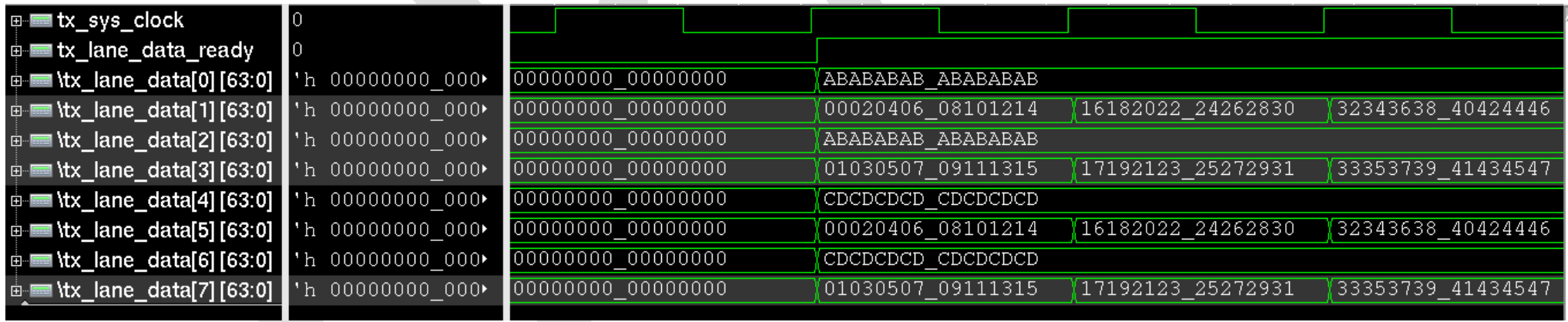
- The transition of
tx_lane_data_readyindicates the Tx IP is ready to start accepting data on all the lanes. - The reader should be able to see a direct 1-1 correlation between the sample ordering on the
tx_lane_databuses and the LMFS table. Each sample is divided among two onsecutive lanes, with the lower numbered lane containing the 8 MSB bits and the higher numbered lane containing the 8 LSB bits.
6.5.2.2 Data mapping with 32 bit and 128 bit Tx IP
The waveforms for the 32bit and 128 bit Tx IPs are not shown, but the sample to lane data mapping remains the same.
- In the 32 bit Tx IP case, the IP will accept 8 samples each of the I and Q channels on each tx_sys_clock cycle
- This is because there are 8 lanes of 32 bits each, resulting in a total of 16 total samples per cycle
- In the 128 bit Tx IP case, the IP will accept 32 samples each of the I and Q channels on each tx_sys_clock cycle
- This is because there are 8 lanes of 128 bits each, resulting in a total of 64 total samples per cycle
6.6 Guidelines for accurate sampling of SYSREF
The SYSREF signal is an integral component of a JESD system, and is used to help synchronize the internal timing of the various Tx and Rx devices in the case of JESD Subclass 1 deterministic latency. Each device is supplied a SYSREF signal and a clock, and the SYSREF is sampled for a positive edge using the provided clock.
The SYSREF signal can have the following characteristics:
- It can be one-shot or periodic or gapped periodic
- The period of the SYSREF must be equal to or an integral multiple of the following:
- The period of the multi-frame in 8b/10b mode
- The period of the extended multi-block in 64b/66b mode
The TI204c IP has features that enable accurate sampling of SYSREF without specific duty cycle constraints being imposed on the SYSREF signal.
- The pulse width of the SYSREF should last for at least one clock cycle. Wider pulses do not change the functionality, as the positive edge of the clock that samples that
0→1transition of the SYSREF is the event used to control the LEMC/LMFC timing in the IP. - In some cases, tight timing constraints may force the addition of one or more sequential stages between the SYSREF at the input pin of the FPGA and the final SYSREF that is passed to the JESD IP. The IP has a feature that can compensate for the offset created by these stages. This is done using the
RX_SYSREF_OFFSETandTX_SYSREF_OFFSETattributes of the IP. - The IP also exports a counter that tracks the number of times that the SYSREF pulse has forced a re-alignment of the LEMC/LMFC timing. This can be used to track cases where the SYSREF frequency isn't an integral multiple of the extended multi-block or multi-frame period.
The following waveform illustrates a case where the RX_SYSREF_OFFSET is set to '1'. The Rx IP has just been released from reset, and its LEMC pulse is out of sync with the Tx LEMC pulse (seen at the TimeA marker in the waveform). The rx_lemc_pulse and tx_lemc_pulse have been highlighted in red for easy reference.
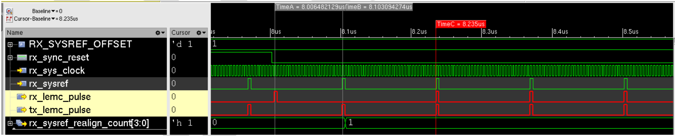
At the point of the second marker (TimeB), the Rx IP re-aligns its internal timing, and the realign counter increments from 'h0 to 'h1. Starting from the third marker (TimeC) the Rx and Tx LEMC pulses are aligned, indicating that the Tx and Rx IP's are honoring the extended multi-block timing of the JESD link. After this point, the rx_sysref_realign_count does not increment again, indicating that the timing of the rx_sysref is in accordance with the timing of the rx_lemc_pulse.
In cases where deterministic latency or synchronization across multiple IP's is not required, the rx_sysref and tx_sysref inputs to the IP can be tied to '0'.
6.7 Synchronizing multiple Rx IPs for simultaneous release of lanes
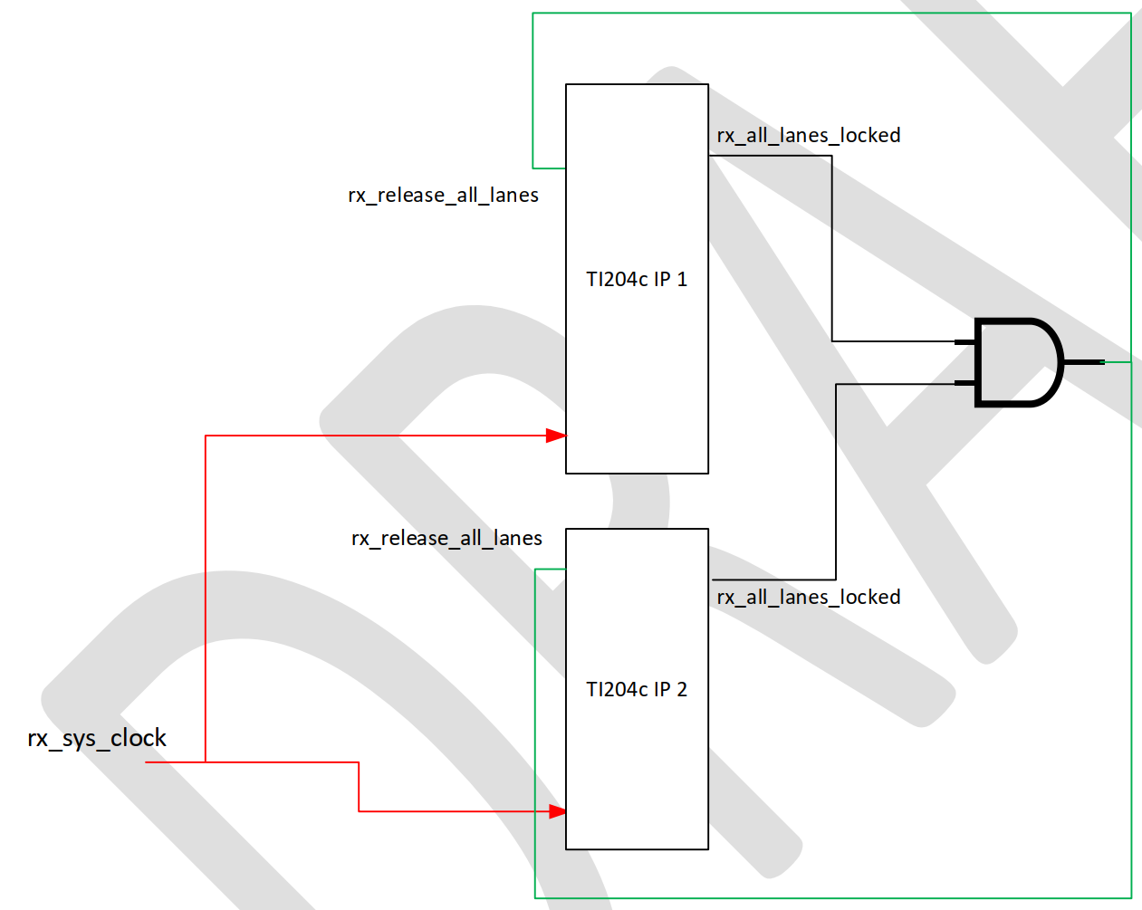
The TI204c IP supports synchronized release across multiple instances of its Rx IP. This is done by monitoring an output signal called "rx_all_lanes_locked", and in turn using it to control the release of the Rx IP's data lanes. The "rx_all_lanes_locked" signal indicates that each individual lane in the IP has aligned to the relevant control / demarcation characters sent by the corresponding Tx / ADC device. This signal is applicable in both 8b/10b as well as 64b/66b modes of operation. However, with multiple Rx IP's in the system, it is possible that each Rx IP completes its locking procedure during a different multiframe or extended multi-block. This can create scenarios where Rx IP's release at different points in time, even though their LEMC/LMFC boundaries are synchronized by using the SYSREF signal.
If there are multiple IP's in a system, the following topology can be used to ensure that all IP's are released simultaneously, even if the lanes in each IP complete their locking at different points in time. This helps simultaneous sampling systems ensure that the data from all channels across multiple devices is aligned in time.
The figure below indicates that all lock status and release control signals are synchronous to the rx_sys_clock clock domain. All lanes of each IP will be released on the next LEMC/LMFC boundary after the input "rx_release_all_lanes" signal has been set to '1' (and the IP has completed locking for all of its lanes).
-
For the above scheme to work reliably, it is important to ensure that all the IP's have aligned to their individual SYSREF signals, which in turn ensures that the IP's are aligned in terms of their multi-frame or extended multiblock boundaries.
-
If there is just one Rx IP in the system, its input "
rx_release_all_lanes" port can be tied to '1'. Alternatively, itsrx_all_lanes_lockedoutput port can be connected back to the "rx_release_all_lanes" input port. -
The
rx_sys_clocksignal (in RED) is shown only for the purpose of illustrating that the "rx_all_lanes_locked" and "rx_release_all_lanes" signals use therx_sys_clockdomain.
- The scheme described above ensures that multiple Rx IP’s release within the same Multi-Frame or Extended Multi-Block boundary. However, while the lanes within an IP will always release together, there may be a variation of +/-1 rx_sys_clock cycles between the data of lanes across the IPs. This is because there may be delay variations across the IPs which result in the samples shifting forward (or back) by 1 rx_sys_clock cycle.
- This variation will not cause system level issues in cases where samples are tracked in the time domain
- For example, if sample 1 of Rx IP 1 has a -1/0/+1 rx_sys_clock relationship to sample 1 of Rx IP 2, this relationship will be maintained across all subsequent samples (until the next time the link is reinitialized).
- However, if it is desired that corresponding samples on all lanes of all Rx IP’s must be aligned to the exact rx_sys_clock cycle, then the scheme described above must be combined with the deterministic latency feature of the TI204c IP (discussed in the next sub-section).
6.8 Implementing Deterministic Latency with the TI204c IP
In both of the cases above, the deterministic latency features enables the designer to absorb and eliminate all the variations in flight time caused by one or more of the following factors:
- Clock domain variations in the ADC/DAC JESD block
- Trace routing/length variations between the data lanes of multiple JESD IPs
- Clock domain variations in the Rx/Tx JESD IPs in the FPGA
- PVT variations across all the components in the entire flight path
At a high level, deterministic latency in a sampling system is implemented by ensuring the following:
- All ADCs and FPGA Rx IPs are aligned in terms of timing
- All ADCs and FPGA Tx IPs in the system are aligned in terms of timing
- In all cases, the release of data on the Rx side should be controlled with a programmable (elastic) buffer that can absorb the variations in the link
- Once the variations are absorbed, there is a deterministic delay to the overall flight time.
6.8.1 Profiling feature for lane release delays (Rx IPs only)
In many cases, determining the variations over the link can be a challenge for the system designer. For the case of ADC based links, the TI204c Rx IP addresses this by introducing a profiling counter that automatically reports the total time delay needed to actually release its lanes (after its rx_release_all_lanes input has transitioned from 0→1).
The value of this counter is reported on one of the following output ports:
rx_lmfc_to_buffer_release_delay(in the case of 8b/10b mode)rx_lemc_to_buffer_release_delay(in the case of 64b/66b mode)
The image below illustrates the functionality of the profiling counter.
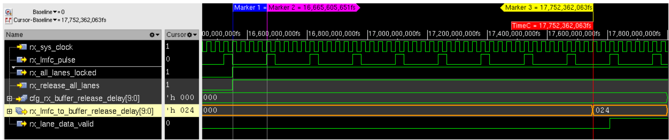
The image contains three markers pertaining to events of significance:
- Marker 1 (blue): This is the point where the Rx IP asserts its "
rx_all_lanes_locked" output signal, which consequently results in the "rx_release_all_lanes" input transitioning from 0 → 1 (explained in section 6.7). - Marker 2 (magenta): This is the subsequent LMFC boundary, where the "
rx_release_all_lanes" is recognized, initiating the lane release process in the Rx IP (and the start of the profiling counter). - Marker 3 (yellow): This is the value of the "
rx_lmfc_to_buffer_release_delay" profiling counter, indicating that it has taken 24h (36 decimal) cycles for the Rx IP to release all the lanes in a simultaneous manner. The "rx_lane_data_valid" activates exactly two cycles later.
If the same release procedure is run multiple times across power cycles and operating conditions, the release value of the profiling counter may show a variation, thereby indicating the spread of how the timing may vary. This spread can then be used to control the exact release time of the lanes, ensuring that there is no further variation.
6.8.2 Deterministic latency for systems containing one ADC and one FPGA Rx IP
The following steps should be followed for implementing robust deterministic latency for a sampling system consisting of one link between an ADC and an FPGA Rx IP.
-
The ADC and Rx IP must be aligned in terms of timing a. This means that they are all reliably sampling their corresponding SYSREF signal with their respective device clocks. i. The procedure for accurate SYSREF sampling by the Rx IP is explained in section 6.6. b. This will ensure that the ADC and FPGA Rx IP in the system are aligned in terms of their frame/multi-frame or multi-block/extended multi-block boundaries.
-
The FPGA Rx IP should have its '
cfg_rx_det_latency_en' signal tied to '1'. -
Connect the '
rx_release_all_lanes' input of the Rx IP as illustrated in section 6.7. a. For a single Rx IP case, it can be a direct connection to the 'rx_all_lanes_locked' output port. -
Force the
cfg_rx_buffer_release_delayinput of the Rx IP to 0x0. -
Determine the release point of the Rx IP using the following steps: a. Keep the Rx IP in reset by forcing its
rx_sync_resetto '1'. b. Release the IP from reset by forcingrx_sync_resetto '0'. If the ADC and Rx IP have been configured correctly, the Rx IP will initialize the link and release its lanes once the 'rx_release_all_lanes' input transitions from '0' to '1' (explained in section 6.7). i. At this point, therx_lmfc_to_buffer_release_delay(8b/10b) orrx_lemc_to_buffer_release_delay(64b/66b) will be updated by the IP. ii. This value reflects the number ofrx_sys_clockcycles needed to release the IP lanes after therx_release_all_lanesevent. c. The following image illustrates these events in time. The buffer release delay value is highlighted in orange. The yellow line indicates the delay from the event that starts the profiling counter.
-
Repeat steps in bullet 5 (above) to determine the spread of the release values for the IP. a. Note: this test should be repeated across power cycles and operating conditions in order to get a representative spread of the timing, as the number may change by a value of up to +/- 20 cycles.
-
Determine the worst case delay number across all tests in step 6, as this will become the limiting delay for guaranteeing deterministic latency.
-
Add a margin value of 2-5 cycles to the worst case delay number obtained in the previous step. For example, if the worst case number was 0x24, the final number (with the added margin) could be any value between 0x26 and 0x29.
-
Force the value of "
cfg_rx_buffer_release_delay" input of the Rx IP to the final value computed in step '8'. -
Run step 5 (above) and ensure that the IP now releases at the fixed delay value. The image below illustrates the result with the "
cfg_rx_buffer_release_delay" value forced to 0x28. It can be seen that the lane profiling counter now releases at the programmed delay.
-
Repeat step 5 across power cycles and operating conditions to ensure that this value does not change.
-
Test the overall flight time in the system by using a pulse at the front end of the ADC and monitoring the samples at the output of the Rx IP. The overall delay should remain constant.
-
You now have deterministic latency in the ADC - Rx IP link.
6.8.3 Deterministic latency for systems containing multiple ADC's and multiple FPGA Rx IP's
The following steps should be followed for implementing robust deterministic latency for a sampling system consisting of multiple ADCs and FPGA Rx IPs. The topology may be any of the following:
- Multiple ADCs connected to one Rx IP (where the Rx IP essentially sees all the ADCs as part of one link)
- Multiple ADCs connected to multiple Rx IP's in one FPGA
- Multiple ADCs connected to multiple Rx IP's across multiple FPGAs
Steps to be followed:
- The ADCs and Rx IP's must all be aligned in terms of timing. a. This means that they are all reliably sampling their corresponding SYSREF signal with their respective device clocks. i. The procedure for accurate SYSREF sampling by the Rx IP is explained in section 6.6. b. This will ensure that all the ADCs and FPGA Rx IPs in the system are aligned in terms of their frame/multi-frame or multi-block/extended multi-block boundaries.
- All FPGA Rx IPs must receive an aligned
rx_sys_clocksignal. a. This will ensure that all FPGA Rx IPs have their individual LEMC/LMFC pulse aligned across one another (depending on the encoding protocol used). - The FPGA Rx IPs should have their '
cfg_rx_det_latency_en' signal tied to '1'. - Connect the '
rx_release_all_lanes' input of all the Rx IPs as illustrated in section 6.7. This will ensure that each Rx IP initiates its lane release procedure at the same aligned LMFC/LEMC boundary. a. Note: This step is extremely important, as different IPs/links may complete their locking procedure at different points in time (and during different multi-frame / extended multi-block periods). - Force the
cfg_rx_buffer_release_delayinput of all Rx IP's to 0x0. - Determine the release point of each Rx IP using the steps explained in section 6.8.2. a. Repeat steps across power cycles and operating conditions to determine the spread of the release values for each IP.
- Determine the worst case delay number across all tests and all IPs in step 6, as this will become the limiting delay for guaranteeing deterministic latency.
- Add a margin value of 2-5 cycles to the worst case delay number obtained in the previous step. For example, if the worst case number was 0x24, the final number (with the added margin) could be any value between 0x26 and 0x29.
- Force the value of
cfg_rx_buffer_release_delayinput of all Rx IP's to the final value computed in step '8'. - Run step 5 (above) and ensure that each IP now releases at the fixed chosen value. a. Repeat steps 5 and 6 across power cycles and operating conditions to ensure that this value does not change.
- Test the overall flight time in the system by using a pulse at the front end of each ADC and monitoring the samples at the output of the corresponding Rx IP. The overall delay should remain constant, both within the link and across links.
- You now have deterministic latency in a multi ADC - multi Rx IP link.
6.8.4 Deterministic latency for systems containing one DAC and one FPGA Tx IP
The following steps should be followed for implementing robust deterministic latency for a sampling system consisting of one link between a DAC and an FPGA Tx IP.
- The DAC and Tx IP must be aligned in terms of timing. a. This means that they are all reliably sampling their corresponding SYSREF signal with their respective device clocks. i. The procedure for accurate SYSREF sampling by the Tx IP is explained in section 6.6. b. This will ensure that the DAC and FPGA Tx IP in the system are aligned in terms of their frame/multi-frame or multi-block/extended multi-block boundaries.
- Force the Tx IP's
tx_sync_resetsignal to '1'. - Force the Tx IP's
tx_sync_resetsignal to '0'. a. The Tx IP will initialize and activate the start and end sideband signals for its lanes. These signals are the frame/multi-frame (8b/10b) or multi-block/extended multi-block signals (64b/66b). b. The relevant data bytes fed to the lanes of the Tx IPs will accordingly be tagged for frame boundaries before being sent to the DAC. c. This enables the data (and samples) to be suitably re-aligned across lanes at the DAC. This alignment is ensured even if multiple lanes across arrive at different points in the time. - At this point, follow the DAC datasheet to ensure a deterministic release of its internal buffers (which will in turn control the timing of the DAC analog outputs).
6.8.5 Deterministic latency for systems containing multiple DACs and multiple FPGA Tx IPs
The following steps should be followed for implementing robust deterministic latency for a sampling system consisting of multiple DACs and FPGA Tx IPs. The topology may be any of the following:
- Multiple DACs connected to one Tx IP (where the Tx IP essentially sees all the DACs as part of one link)
- Multiple DACs connected to multiple Tx IP's in one FPGA
- Multiple DACs connected to multiple Tx IP's across multiple FPGAs
The following steps should be followed for implementing robust deterministic latency for a sampling system consisting of multiple links between DACs and FPGA Tx IPs.
- The DACs and Tx IP's must all be aligned in terms of timing. a. This means that they are all reliably sampling their corresponding SYSREF signal with their respective device clocks. i. The procedure for accurate SYSREF sampling by the Tx IP is explained in section 6.6. b. This will ensure that all the DACs and FPGA Tx IPs in the system are aligned in terms of their frame/multi-frame or multi-block/extended multi-block boundaries.
- All FPGA Tx IPs must receive an aligned
tx_sys_clocksignal. a. This will ensure that all FPGA Tx IPs have their individual LEMC/LMFC pulse aligned across one another (depending on the encoding protocol used). - All FPGA Tx IPs must receive sample/lane data that is aligned (in order for the samples to be re-aligned when extracted at the Rx end). The steps for this are: a. Monitor the LEMC/LMFC pulses across all Tx IPs to ensure that they are aligned in edge as well as phase. b. Ensure that samples that need to remain aligned through the JESD link are fed to the Tx IPs in an aligned manner. i. This is carried out by ensuring that the samples received by the various lanes of the Tx IP's on a frame/multi-frame/multi-block/extended multi-block boundary are all aligned. ii. The relevant data bytes fed to the lanes of the all Tx IPs will accordingly be tagged for frame boundaries before being sent to the DAC. iii. This enables the data (and samples) to be suitably re-aligned across lanes at the DAC. This alignment is ensured even if multiple lanes across arrive at different points in time.
- At this point, follow the DAC datasheet to ensure a deterministic release of its internal buffers (which will in turn control the timing of the DAC analog outputs).
- You will now have deterministic latency across all the DAC - Tx IP links in the system.
7 Timing Constraint Guidelines
The TI204c JESD IP has been architected to simplify the definition of timing constraints, and also minimize the overall P&R effort and runtime incurred by the Vivado tools. The following table lists the primary ports that need timing constraints and the associated guidelines.
Note: In addition to the table below, it is recommended that the designer use the constraints file provided with the customized reference design as the primary starting point for specification of timing constraints.
mgt_refclk_p
- Constraint type: Clock
- Guidelines: Define a clock on this port with the appropriate frequency.
mgt_freerun_clock
- Constraint type: Clock
- Guidelines: Define a clock on this port with the appropriate frequency.
master_reset_n
- Constraint type: False Path
- Guidelines: The master reset is asynchronous and should be set as false path.
rx_sync_clock
- Constraint type: Clock and False Paths
- Guidelines:
- Define a clock on this port with the appropriate frequency.
- Define
rx_sync_clockandmgt_freerun_clockas asynchronous to each other.
tx_sync_clock
- Constraint type: Clock
- Guidelines:
- Define a clock on this port with the appropriate frequency.
- Define
tx_sync_clockandmgt_freerun_clockas asynchronous to each other.
mgt_rx_usrclk2 domain
- Constraint type: Multi-cycle paths
- Guidelines: Set a multi-cycle path of 50ns with the –datapathonly option for all paths between
mgt_rx_usrclk2andrx_sync_clock. This constraint is necessary only if theRX_BUFFER_TYPEattribute is set to "NORM".
mgt_tx_usrclk2 domain
- Constraint type: Multi-cycle paths
- Guidelines: Set a multi-cycle path of 50ns with the –datapathonly option for all paths between
mgt_tx_usrclk2andtx_sync_clock. This constraint is necessary only if theTX_BUFFER_TYPEattribute is set to "NORM". If the attribute is set to "NONE", this constraint should be excluded.
cfg_*
- Constraint type: False Paths
- Guidelines: All inputs to the IP with the name
cfg_*can be set as false paths. This is because they need to be held static before the IP is released from reset.
rx_release_all_lanes
- Constraint type: Multi-cycle Path
- Guidelines: This signal is generated by ANDing all of the
rx_all_lanes_lockedsignals of various IP's (as described in section 6.7). While both signals lie in therx_sys_clockclock domain, therx_all_lanes_lockedoutput is aligned to an LEMC/LMFC pulse boundary, and therx_release_all_lanesinput is not sampled until the next LEMC/LMFC pulse boundary. This creates a multi-cycle path that can be specified if Rx synchronization signals are being passed across FPGA / SLR boundaries and timing closure is a challenge at the targetedrx_sys_clockfrequency.
8 TI204c-IP Reference Designs
The TI204c-IP archive includes a number of reference designs based on standard development kits offered by Xilinx. These designs can be used in the following ways:
- They can be ported to other FPGAs of your choice (with necessary modifications)
- They can be used as a starting reference point for a completely customized JESD solution
- Components of the testbench can be used as functional models for simulations. For example, an Rx only JESD IP can use the Tx part of the reference design as the JESD transmitter model to validate the link in simulations.
All the components of the reference design (except the TI204c-IP core) are un-encrypted and can be edited for further customization.
8.1 Reference design block diagram
The block diagram below illustrates the general structure of the reference design provided to you. The reference design implements a full duplex JESD link with both the Tx and Rx IP's configured to the same JESD link parameters.
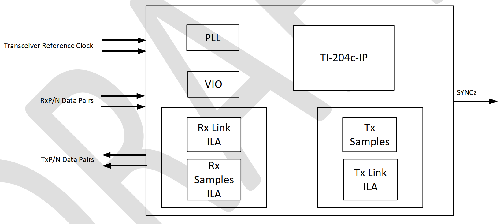
The reference design can be broken down into the following primary functional blocks:
- The TI204c JESD IP core : This is the IP configured for the targeted mode of operation.
- PLL : this is an FPGA PLL that is used to generate all the internal clocks in the design.
- VIO (virtual input output) module : This is a visibility/control module that enables the following:
- Control of signals feeding into the IP. These are primarily the resets of the JESD IP.
- Reading of static outputs from the IP. These include transceiver QPLL/CPLL/CDR locked status signals.
- Rx Reference Design
- Rx Link ILA (internal logic analyzer). This captures the Rx lane and sideband signals.
- Rx Samples ILA : This captures the Rx lane data mapped to ADC samples.
- Rx ILAS VIO (8b/10b modes only): This VIO captures the ILAS configuration octets captured by the receiver during the lane initialization sequence of the 8b/10b JESD link.
- Tx Reference Design
- Tx samples : This logic generates a simple 64 point sine/cosine wave that is fed to the Tx IP.
- Tx Link ILA (internal logic analyzer). This captures the Tx lane data and sideband signals.
8.1.1 Reference Design Datapaths
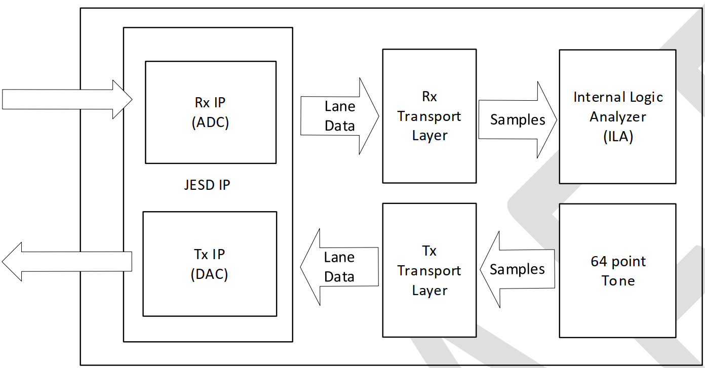
The primary Tx and Rx datapaths consists of the following sub-modules:
- Rx IP (ADC) Data-path
- The JESD Rx IP. This is part of the TI204c JESD IP Core.
- The Rx Transport Layer. This logic maps the lane data to samples.
- Samples buffer. This is implemented using an internal logic analyzer. The captured samples can be exported to a CSV file using Vivado.
- Tx IP (DAC) Data-path
- The JESD Tx IP. This is part of the TI204c JESD IP Core.
- 64 point tone. This module generates samples that emulate 16bit 64 point sine/cos tones. The samples can be attenuated in amplitude by a factor of 1/2/4 and 8.
- The Tx Transport Layer. This logic maps the samples to the lane data that is received by the JESD Tx IP.
8.1.2 Reference Design Loopback Test Environment
The Reference designs have been architected to have the Tx and Rx IP's connected in a loopback fashion to generate a standalone system that does not need to interface with an actual ADC / DAC / AFE EVM or simulation model. The loopback connections are illustrated in the following figure.
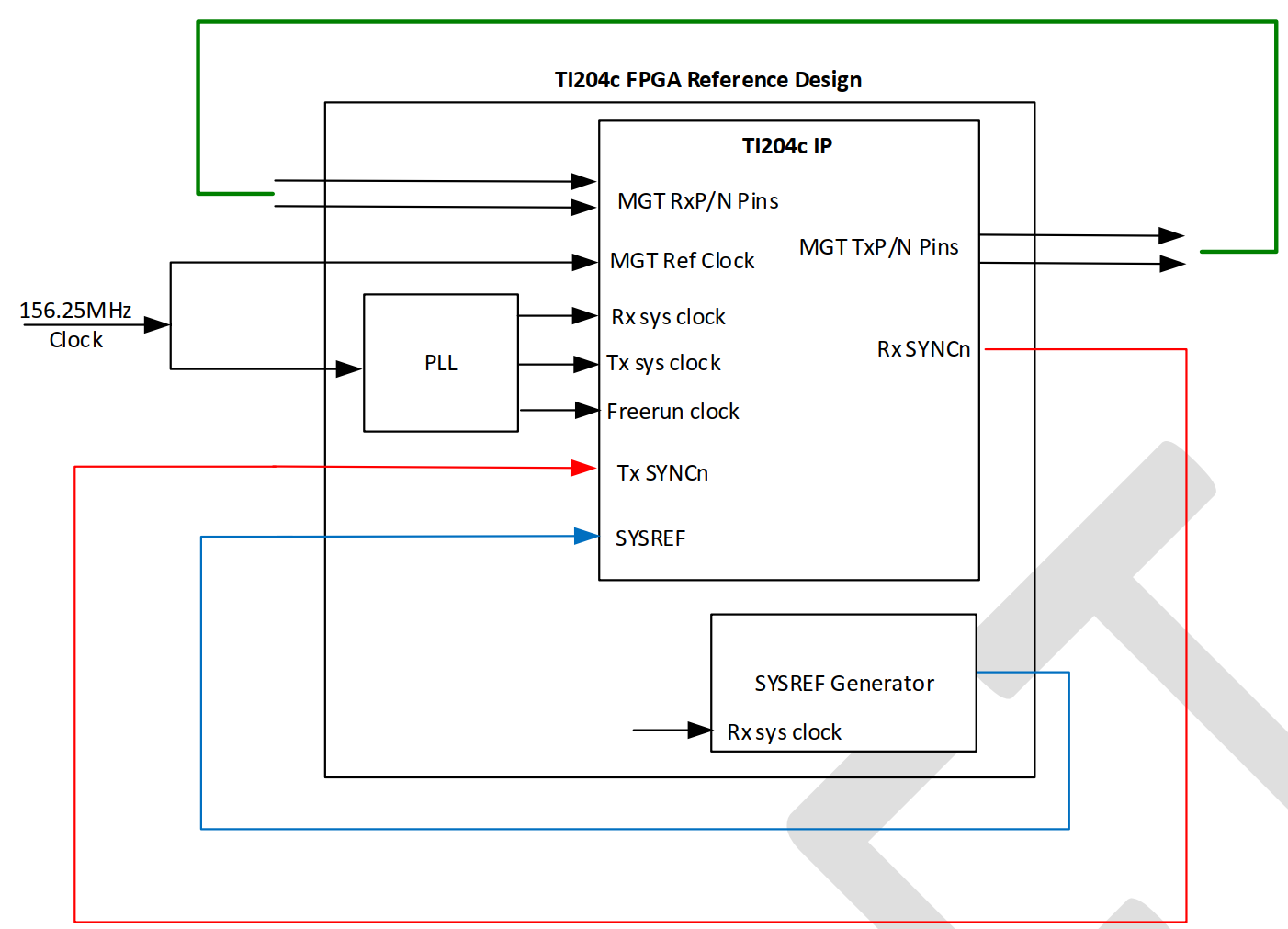
The primary loopback paths are illustrated in various colors in the figure above, and the details of the same are listed in the following points:
- There is a 1-1 loopback on all the Tx and Rx lanes. For example, Tx[0] is mapped to Rx[0], Tx[1] is mapped to Rx[1], and so on.
- The Rx SYNCn signal is looped back to the Tx SYNCn signal. This is applicable only in the case of 8b/10b designs.
- The SYSREF Generator block emulates the typical functionality of a clocking chip, and the SYSREF is looped back to the corresponding input of the Tx and Rx IPs. For the purpose of accurate timing, the SYSREF is generated using the same clock that is connected to the
rx_sys_clockandtx_sys_clockinputs of the JESD IP core.
8.1.2.1 Reference Design Loopback Hardware
The reference designs implement loopback using a Whizz Systems XM107 FMC loopback test card. The link to the card schematics can be found in section 9 of this user guide.
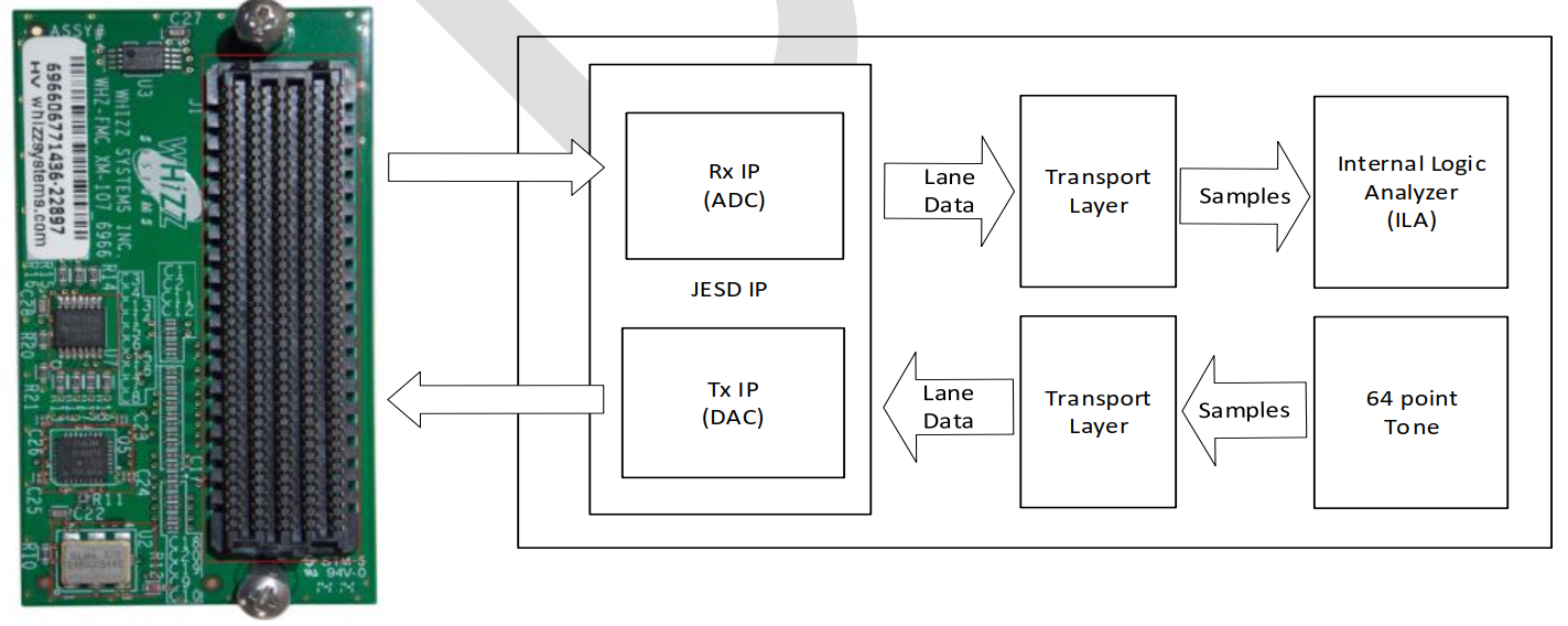
8.2 Reference Design List
The TI204c IP reference designs have been categorized based on the transceiver architecture (GTP/GTY/GTH/GTX) instead of FPGA families. This is because multiple FPGA parts across different families may contain a certain class of transceiver. As a result, a reference design based on that class can easily be ported to any target FPGA containing that particular transceiver.
The table below lists all the reference designs included with the TI204c IP archive. The last column in the table lists the possible FPGAs that each reference design can map to.
| Protocol | Reference Design Name | Lane Rate | DevKit | LMFS | K/E | Transceiver Class | Target FPGAs |
|---|---|---|---|---|---|---|---|
| 8b/10b | zcu102_8b10b | 12.5 Gbps | zcu102 | 8-8-2-1 | 32 | GTH | Zynq UltraScale+, Kintex UltraScale+, Virtex UltraScale, Kintex UltraScale, Virtex-7 |
| vcu118_8b10b | 12.5 Gbps | vcu118 | 8-8-2-1 | 32 | GTY | Virtex UltraScale+, Kintex UltraScale+, Zynq UltraScale+ | |
| zc706_8b10b | 6.25 Gbps | zc706 | 8-8-2-1 | 32 | GTX | Kintex-7, Zynq7000, Virtex-7, Artix-7* | |
| 64b/66b | zcu102_64b66b | 10.3125 Gbps | zcu102 | 8-8-2-1 | 3 | GTH | Zynq UltraScale+, Kintex UltraScale+, Virtex UltraScale, Kintex UltraScale, Virtex-7 |
| vcu118_64b66b | 10.3125 Gbps | vcu118 | 8-8-2-1 | 3 | GTY | Virtex UltraScale+, Kintex UltraScale+, Zynq UltraScale+ | |
| vcu118_64b66b_2 | 20.625 Gbps | vcu118 | 4-8-4-1 | 3 | GTY (128 bit) | Virtex UltraScale+, Kintex UltraScale+, Zynq UltraScale+ | |
| zc706_64b66b | xx | zc706 | - | - | GTX | Refer notes below |
There are a few important things that need to be noted:
- Mapping between Transceivers and FPGAs
- A particular class of FPGAs may contain more than one class of transceivers. For example the Kintex UltraScale+ family can contain both GTH and GTY class transceivers.
- A particular class of transceivers may be present in more than one FPGA family. For example, the GTH class transceiver can be found in Zynq UltraScale+, Kintex UltraScale+, Kintex UltraScale as well as Virtex7 families.
- Always ensure that you select the reference design based on the transceiver class that is connected to the dataconverter.
- The GTX class reference design also applies for the GTP transceivers (found on Artix-7 FPGAs).
- The
vcu118_64b66b_2reference design demonstrates the 128 bit/lane capability of the JESD IP. This allows extremely high lane rates while keeping the user logic clock rates low, thus enabling easier timing closure constraints. - The
gtx_8b10breference design uses anrx_sys_clockof 156.25MHz, while the requiredrx_sys_clockis 78.125MHz. This design showcases the ability of the Rx JESD IP to maintain an accurate data output by using thelane_data_validsignal to indicate when the lane data is to be honored/discarded. This functionality is explained in section 6.4.7. - While this is not explicitly listed, TI does support 64b/66b solutions for the GTX class transceivers. However, this is a very customized solution and you are requested to reach out to TI support for a special delivery of the same.
8.3 Reference Design Hierarchy
Each reference design implements a standard hierarchy (as illustrated below). The TI204c IP core is the encrypted JESD IP, and the rest of the modules are part of the reference design. The entire Reference Design is functional when compiled stand-alone for an FPGA, and does not need any additional logic.
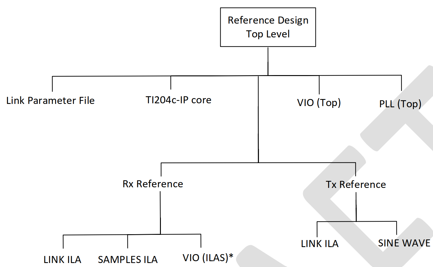 *
Notes:
- The 'Link Parameter File' is a .vh (Verilog header/include) file that essentially sets all the customization parameters of the TI204c-IP core for the reference design.
- Most of the functionality of the TI204c-IP can be modified / controlled by editing this parameter file.
- There is an extra VIO provided in the Rx reference design, and is instantiated only in 8b/10b mode. This VIO captures the 14 ILAS config octets received by the Rx IP during the ILAS sequence of the link bring-up phase.
- The LINK ILA and the VIO (ILAS) have a limit of capturing relevant data for up to 8 lanes. This has been kept limited to 8 to reduce the resource usage in the FPGA, but if necessary it can be modified to account for IP's with a larger number of lanes.
- The Tx LINK ILA has a limit of capturing relevant data for up to 8 lanes. This has been kept limited to 8 to reduce the resource usage in the FPGA, but if necessary it can be modified to account for IP's with a larger number of lanes.
8.4 Core IP Archive File Structure
The directory structure of the Core IP archive is illustrated in the figure below.
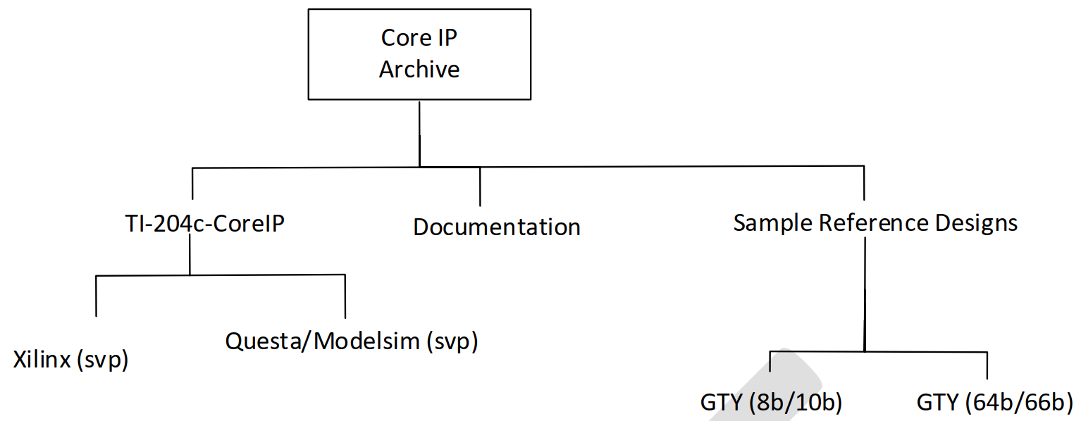
Notes:
- The TI204c-IP design contains two primary directories:
- The JESD IP core. This is provided as an encrypted svp file. There are two flavors of the encrypted svp file of the TI204c-IP core:
TI204c-IP_xilinx.svp: meant for all Vivado based tool flowsTI204c-IP_questasim.svp: meant for Questa/Modelsim simulations
- Example Reference Designs
- These directories contain all the files (except the JESD IP core) needed for compilation and bit-file generation.
- The JESD IP core. This is provided as an encrypted svp file. There are two flavors of the encrypted svp file of the TI204c-IP core:
8.5 Loading the Reference design in Vivado
Launch Vivado (2019.x or higher) and open a new project with the name of your choice.
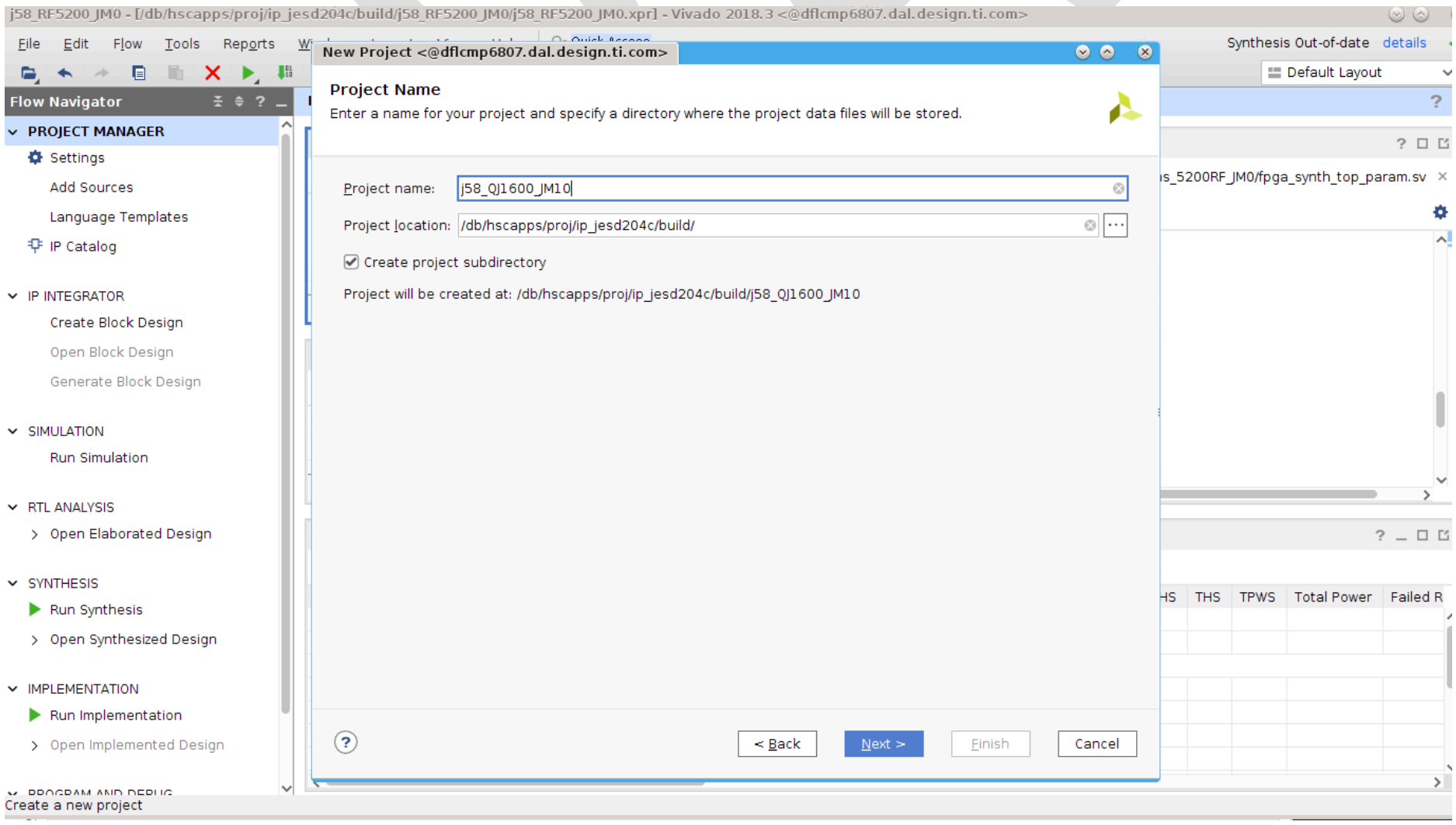 Set the FPGA part number by selecting the targeted DevKit listed in section for the chosen reference design (8.2).
- Read the following design/source files into Vivado:
- The
TI_204c_IP_xilinx.svpfrom the CoreIP RTL directory. - All the .sv, .vh and .xci files provided in the Reference Design Directory.
- Remember to exclude the Questa/Modelsim svp file, as it is meant only for simulations.
- The
- Set the top level to
TI_204c_IP_ref(this should get set automatically by Vivado). - Read the provided constraints file and set it as the target.
- For the Xilinx IP, a few additional steps may need to be carried out:
- If the IP shows a 'locked' status, right-click and select Upgrade IP, leaving core container disabled.
This step will load all the necessary files of the reference design into Vivado and link across the modules to indicate if any instances lack a reference module. The design flow can now be executed to generate the bitfile for the reference design.
8.6 Testing the Reference Design
The bitfile generated for the reference design can be tested using the following steps:
- Install the Whizz loopback card on the FMC connector of the targeted Xilinx DevKit board.
- Program the FPGA with the bitfile.
- The VIO in the reference design is set up to keep the JESD IP in reset when the FPGA completes programmation.
- The master reset signal (
master_reset_n) is held to its active value '0'. - The individual Rx/Tx IP resets (
rx_sync_reset_vio/tx_sync_reset_vio) are held to the active value '1'.
- The master reset signal (
- Steps to release the JESD IP (using the VIO):
- Set the
master_reset_nsignal to '1'. - The QPLL0 locked signals should now all read as '1' (indicating that the transceiver PLL is generating the targeted line rate).
- Set the
tx_sync_reset_viosignal to '0'. This releases the Tx JESD IP from reset and it starts transmitting data over all the lanes. - Set the
rx_sync_reset_viosignal to '0'. This releases the Rx JESD IP from reset.
- Set the
- Once the above steps are complete the JESD Rx IP is expected to lock into the data stream from the Tx, and all the lanes are released in a synchronized manner at the multi-frame or extended multi-block boundary.
- The values exported by the lanes (and the relevant error signals) can be monitored using the ILA provided in the reference design.
- The samples extracted from the lane data can be monitored using the SAMPLES ILA instance in the reference design.
- The reference design also contains support for testing deterministic latency (as described in Section 6.8).
- The
cfg_rx_buffer_release_delayandrx_lcmc/lmfc_to_buffer_release_delaysignals are mapped to the VIO for calibrating and fixing the deterministic delay of the link.
- The
8.7 Mapping the reference design to a different FPGA or DevKit
Once the reference design has been compiled and tested on the original supported DevKit, it can now be transitioned to any other FPGA or DevKit using the following steps:
- Open the transceiver wizard and note down all the settings on all the pages of the wizard. This will be important in step (4) below, because the same settings will need to be created for the transceiver on the new FPGA.
- Save the original tested project as a new project with the new FPGA / DevKit set as the target device/board. Choose the option to copy all the source files, IPs and constraints.
- Vivado may lock the IPs when the new project is created, but they can be upgraded using the same steps as listed in the steps for loading and compiling the original reference design.
- Important: While most Xilinx macro IPs port seamlessly across FPGA families, the same does not apply for the transceivers. In this case, it is important that you create a new transceiver IP using the transceiver wizard. The settings saved in Step 1 must be used as a reference to generate the new transceiver IP.
- Your project should now be ready for compilation on the targeted FPGA/board.
9 References
- JESD204C JEDEC Standard (jede.c.org)
- GTH Transceivers User Guide (Xilinx.com)
- GTY Transceivers User Guide (Xilinx.com)
- Xilinx UltraScale Transceiver Wizard (Xilinx.com)
- Please refer to other FPGA related datasheets and user guides on Xilinx.com
- Please refer to ti.com for datasheets pertaining to all the TI dataconverters
- Whizz Systems FMC loopback test card
10 Revision History
| Version | Author | Date | Description |
|---|---|---|---|
| 1.00 | Ameet Bagwe | 11/29/2020 | First official release of the TI204c JESD IP |
| 1.01 | Ameet Bagwe | 01/07/2021 | Changes to Documentation • Corrected clock domain for rx_lane_buffer_overflow output port• Included Section for aligned / synchronized release of multiple Rx IP's |
| 1.02 | Ameet Bagwe | 02/16/2021 | Changes to Documentation • Included Section for Deterministic Latency Changes to Design • Datapath to rx_sync_n output port optimized for tighter timing control |
| 1.03 | Ameet Bagwe | 02/24/2021 | Changes to Documentation • Updated Section 6.7 (Deterministic Latency) with more details Changes to Design • Lane release delay output logic modified to mask intermediate values of the profiling counter • No change to primary functionality of the IP |
| 1.10 | Ameet Bagwe | 05/18/2021 | Changes to Design • New parameter “ RX_BUFFER_RATIO” added to IP. Reserved functionality• New test ports added to IP. Reserved functionality • All internal buffers/FIFO's modified from XCI based macros to synthesizable XPM primitives • New reference designs included with IP core archive Changes to Documentation • Updated Parameter and Port list with new parameter and test ports • Added Transceiver Wrapper and Instantiation Guidelines (Section 6.1) • Updated Sections 6.8.4 and 6.8.5 for DAC related care-about for deterministic latency • Added Section 8 for new reference designs included with IP core archive |