Zynq UltraScale+ XCZU7EV MPSoC
[Figure 2-1, callout 1]
The ZCU106 board is populated with the Zynq UltraScale+ XCZU7EV-2FFVC1156 MPSoC, which combines a powerful processing system (PS) and programmable logic (PL) in the same device. The PS in a Zynq UltraScale+ MPSoC features the Arm® flagship Cortex®-A53 64-bit quad-core processor and Cortex-R5F dual-core real-time processor.
Production ZCU106 evaluation boards will ship with -2 speed grade devices. Support of multiple speed grades requires voltage adjustments.
The VCCINT supplies are user adjustable via the PMBus with the voltage ranges listed in Table 3-1 to support multiple Zynq UltraScale+ MPSoC speed grades.
Table 3-1: Recommended Operating Conditions
| Symbol | Description | Min | Typ | Max | Units |
|---|---|---|---|---|---|
| Processing System | |||||
| VCC_PSINTFP | PS full-power domain supply voltage. | 0.808 | 0.850 | 0.892 | V |
| For -1LI and -2LE (VCCINT = 0.72V) devices: PS full-power domain supply voltage. | 0.808 | 0.850 | 0.892 | V | |
| For -3E devices: PS full-power domain supply voltage. | 0.873 | 0.900 | 0.927 | V | |
| VCC_PSINTLP | PS low-power domain supply voltage. | 0.808 | 0.850 | 0.892 | V |
| For -1LI and -2LE (VCCINT = 0.72V) devices: PS low-power domain supply voltage. | 0.808 | 0.850 | 0.892 | V | |
| For -3E devices: PS low-power domain supply voltage. | 0.873 | 0.900 | 0.927 | V | |
| Programmable Logic | |||||
| VCCINT | PL internal supply voltage. | 0.825 | 0.850 | 0.876 | V |
| For -1LI and -2LE (VCCINT = 0.72V) devices: PL internal supply voltage. | 0.698 | 0.720 | 0.742 | V | |
| For -3E devices: PL internal supply voltage. | 0.873 | 0.900 | 0.927 | V | |
The top-level block diagram is shown in Figure 3-1.
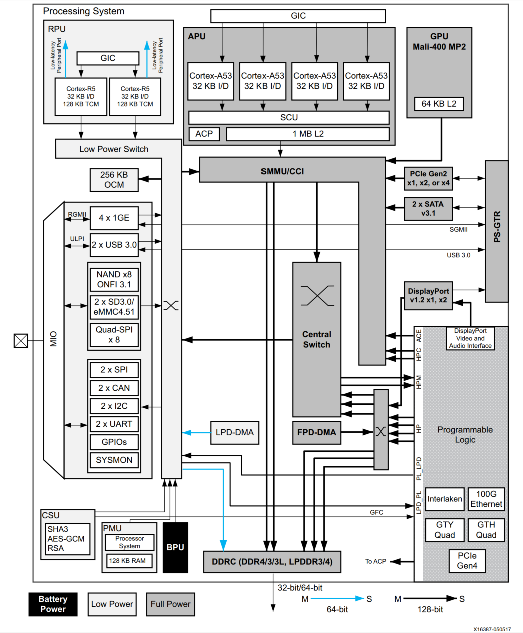
The Zynq UltraScale+ MPSoC PS block has three major processing units:
- Cortex-A53 application processing unit (APU) - Arm v8 architecture-based 64-bit quad-core multiprocessing CPU.
- Cortex-R5F real-time processing unit (RPU) - Arm v7 architecture-based 32-bit dual real-time processing unit with dedicated tightly coupled memory (TCM).
- Mali-400 graphics processing unit (GPU) - graphics processing unit with pixel and geometry processor and 64 KB L2 cache.
The Zynq UltraScale+ MPSoC PS has four high-speed serial I/O (HSSIO) interfaces supporting these protocols:
- Integrated block for PCI Express® interface - PCIe™ base specification version 2.1 compliant.
- SATA 3.1 specification compliant interface.
- DisplayPort interface - implements a DisplayPort source-only interface with video resolution up to 4K × 2K - 30 (300 MHz pixel rate).
- USB 3.0 interface - compliant to USB 3.0 specification implementing a 5 Gb/s line rate.
- Serial GMII interface - supports a 1 Gb/s SGMII interface.
The PS and PL can be coupled with multiple interfaces and other signals to effectively integrate user-created hardware accelerators and other functions in the PL logic that are accessible to the processors. They can also access memory resources in the PS. The PS I/O peripherals, including the static/flash memory interfaces share a multiplexed I/O (MIO) of up to 78 MIO pins. Zynq UltraScale+ MPSoCs can also use the I/O in the PL domain for many of the PS I/O peripherals. This is done through an extended multiplexed I/O interface (EMIO) and boots at power-up or reset.
For additional information on Zynq UltraScale+ MPSoC devices, see the Zynq UltraScale+ MPSoC Data Sheet: Overview (DS891) . See the Zynq UltraScale+ MPSoC Technical Reference Manual (UG1085) for more information about Zynq UltraScale+ MPSoC configuration options.
Encryption Key Battery Backup Circuit
The XCZU7EV MPSoC U1 implements bit stream encryption key technology. The ZCU106 board provides the encryption key backup battery circuit shown in Figure 3-2.
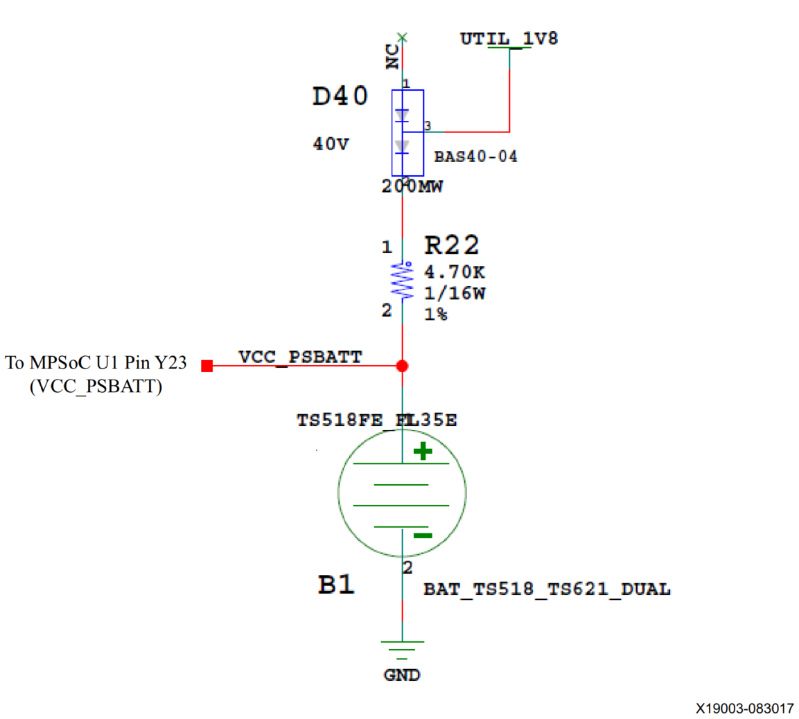
The Seiko TS518FE rechargeable 1.5V lithium button-type battery B1 is soldered to the board with the positive output connected to the XCZU7EV MPSoC U1 Vcc_PSBATT pin Y23. The battery supply current IBATT specification is 150 nA maximum when board power is off. B1 is charged from the UTIL_1V8 1.8V rail through a series diode with a typical forward voltage drop of 0.38V and 4.7Ω current limit resistor. The nominal charging voltage is 1.42V.
On MPSoC devices, the encryption key battery is also used for the battery-backed RAM and the real-time clock (RTC) supply voltage. See the Zynq UltraScale+ MPSoC Data Sheet: DC and AC Switching Characteristics (DS925) [Ref 2].
I/O Voltage Rails
The XCZU7EV MPSoC PL I/O bank voltages on the ZCU106 board are listed in Table 3-2.
Table 3-2: I/O Voltage Rails
| XCZU7EV | Power Net Name | Voltage | Connected To |
|---|---|---|---|
| PL Bank 28 | VADJ_FMC(1) | 1.8V | FMC_HPC1 LA BUS, PMOD0 |
| PL Bank 64 | VCC1V2 | 1.2V | DDR4 DQ[0:31] |
| PL Bank 65 | VCC1V2 | 1.2V | DDR4 DQ[32:63] |
| PL Bank 66 | VCC1V2 | 1.2V | DDR4 ADDR/CTRL, GPIO LED, GPIO SW, PMOD1 |
| PL Bank 67 | VADJ_FMC(1) | 1.8V | FMC_HPC0 LA BUS, GPIO DIP SW |
| PL Bank 68 | VADJ_FMC(1) | 1.8V | FMC_HPC0 LA BUS, SFP REC CLOCK |
| PL Bank 87 | VCC3V3 | 3.3V | HDMI, MSP430 GPIO |
| PL Bank 88 | VCC3V3 | 3.3V | TRACE DEBUG CONNECTOR |
| PS Bank 500 | VCCOPS | 1.8V | CAN, UART0/1, I2C0/1, QSPI LWR/UPR |
| PS Bank 501 | VCCOPS | 1.8V | SDIO, PMU_GPO[0:5], DP |
| PS Bank 502 | VCCOPS | 1.8V | ENET, USB_DATA[0:7], USB_CTRL |
| PS Bank 503 | VCCOPS3 | 1.8V | PS CONFIG I/F |
| PS Bank 504 | VCCO_PSDDR_504 | 1.2V | DDR4 SODIMM I/F |
Notes:
- The ZCU106 board is shipped with VADJ_FMC set to 1.8V by the MSP430 system controller.